A. What are Wafer Handling Arms?
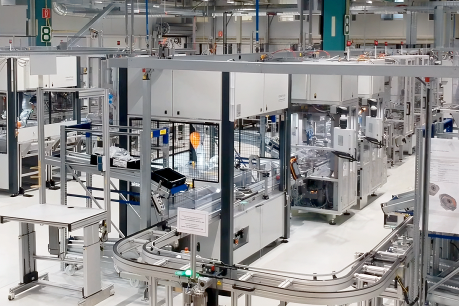
Wafer handling arms, also known as end effectors or wafer blades, are robotic components designed to safely grip, transport, and position silicon wafers during semiconductor manufacturing processes. These precision-machined arms operate in ultra-clean environments within automated material handling systems (AMHS), transferring wafers between processing equipment, load ports, and storage cassettes. Critical to maintaining wafer integrity, these arms must provide gentle yet secure handling while generating minimal particles. They are essential in 200mm and 300mm wafer fabs, enabling high-throughput production in applications ranging from lithography and deposition to inspection and testing stations across the semiconductor supply chain.
B. Principais requisitos técnicos
Wafer handling arms CNC machining demands extraordinary precision with tolerances typically held to ±0.0005″ (±0.0127mm) or tighter for critical dimensions. Flatness specifications often require less than 0.001″ across the entire blade surface to prevent wafer warpage or slippage. Surface finish requirements are stringent, with Ra values below 32 microinches (0.8 μm) and often below 16 microinches to minimize particle generation and adhesion points.
Materials must exhibit excellent dimensional stability across temperature fluctuations (typically 20-25°C in fabs), low outgassing properties for vacuum compatibility, and resistance to cleaning chemicals including IPA, acetone, and piranha solutions. Load-bearing capacity must support 300mm wafers (up to 125g) with deflection under 0.1mm at maximum extension. Electrostatic discharge (ESD) protection and non-magnetic properties are often specified for sensitive fabrication environments.
C. Desafios e soluções para o fabrico
Machining wafer handling arms presents unique challenges due to their thin, flat geometry prone to distortion during cutting operations. Maintaining flatness while achieving tight tolerances across extended blade lengths requires specialized fixturing and low-stress clamping techniques. Material selection adds complexity—aluminum alloys demand different cutting strategies than engineered polymers, each requiring optimized feeds, speeds, and tool geometries to prevent surface defects or dimensional drift.
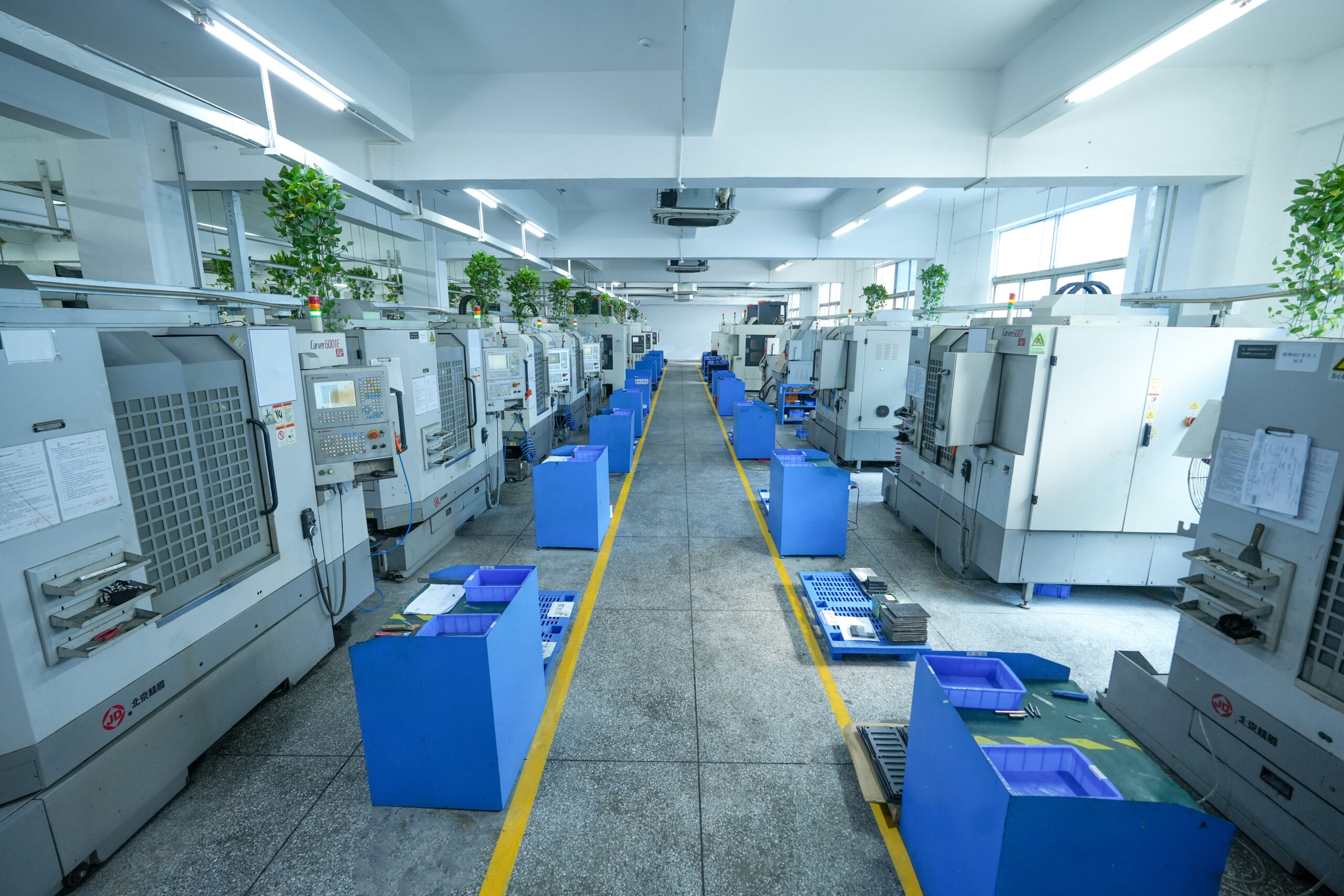
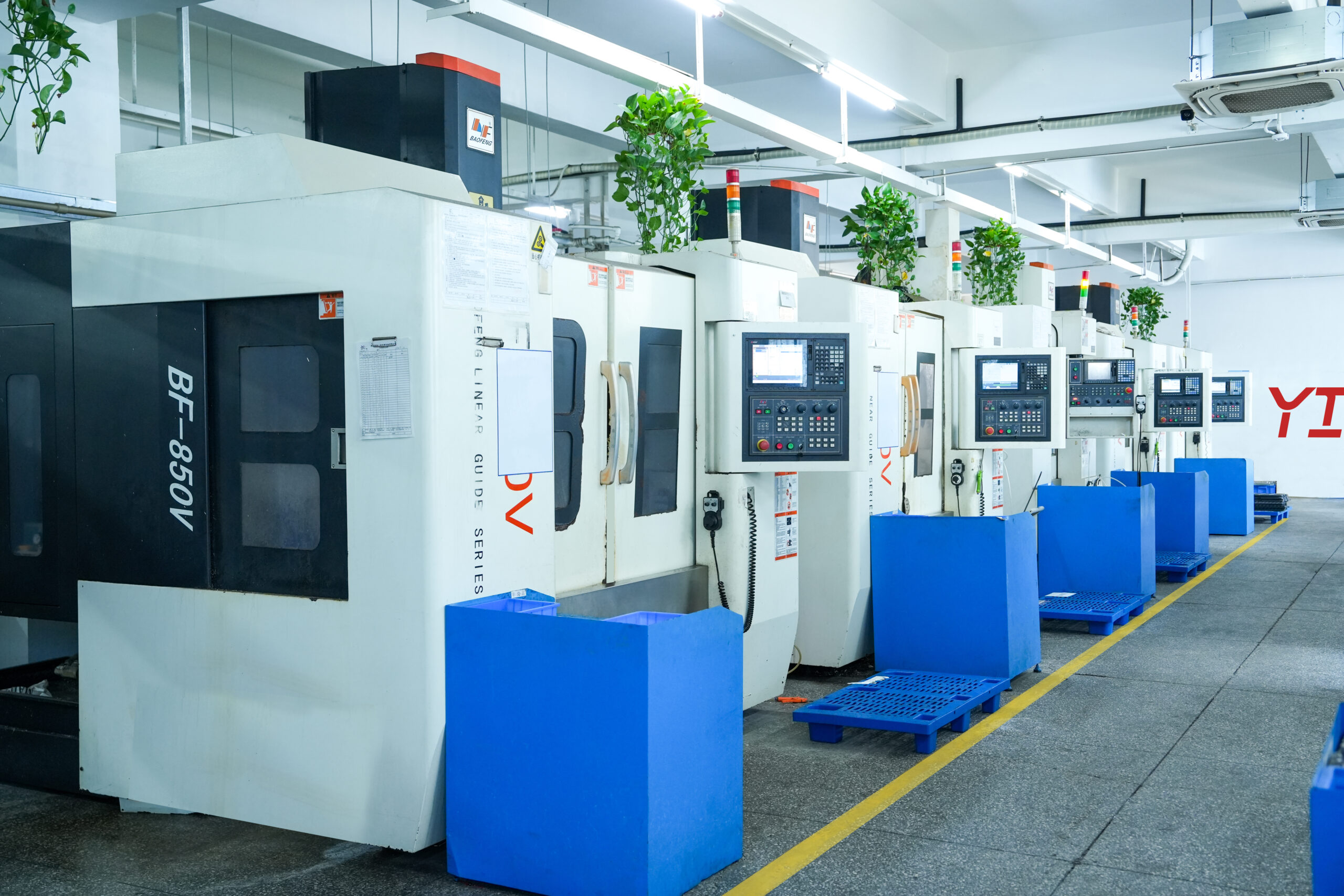
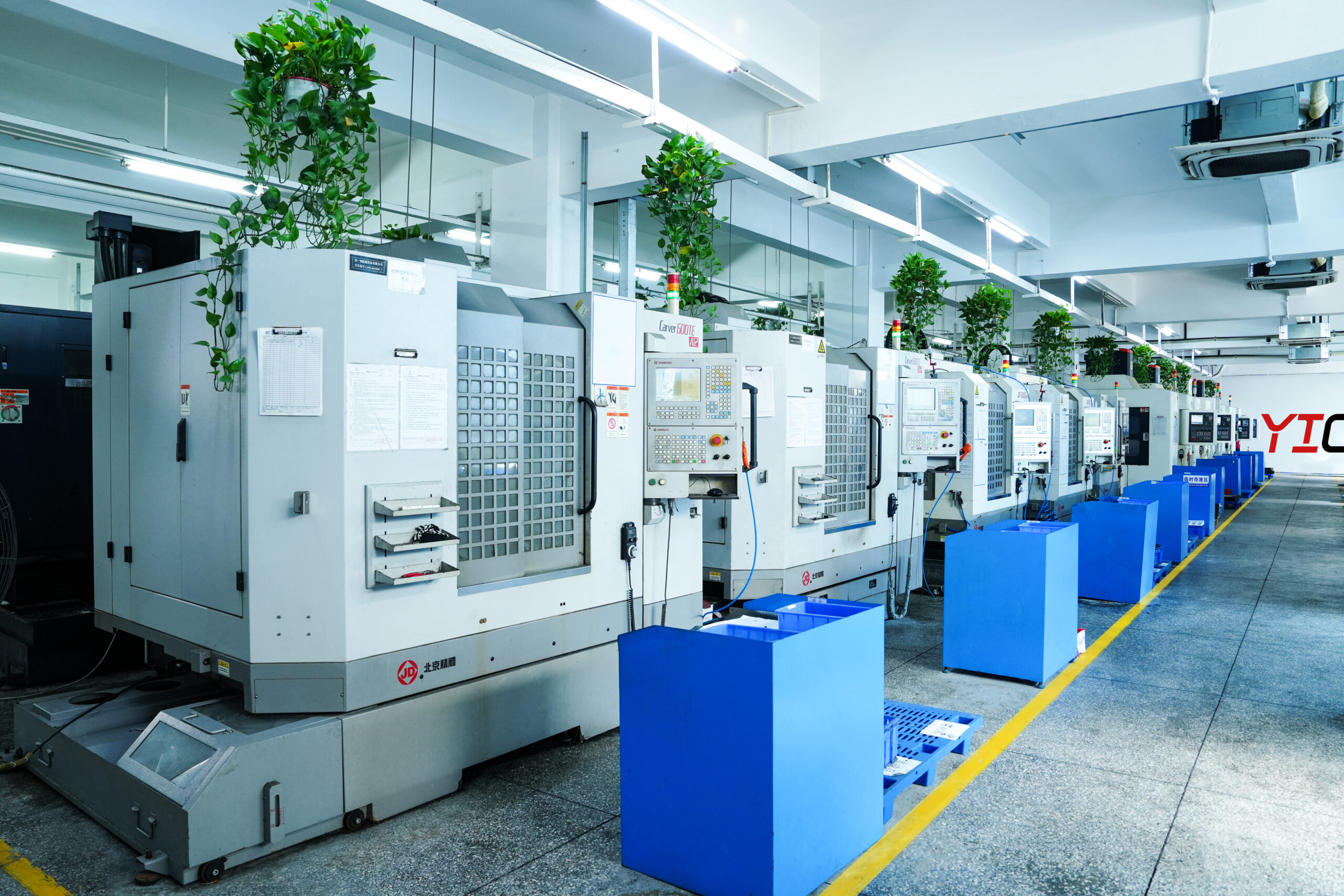
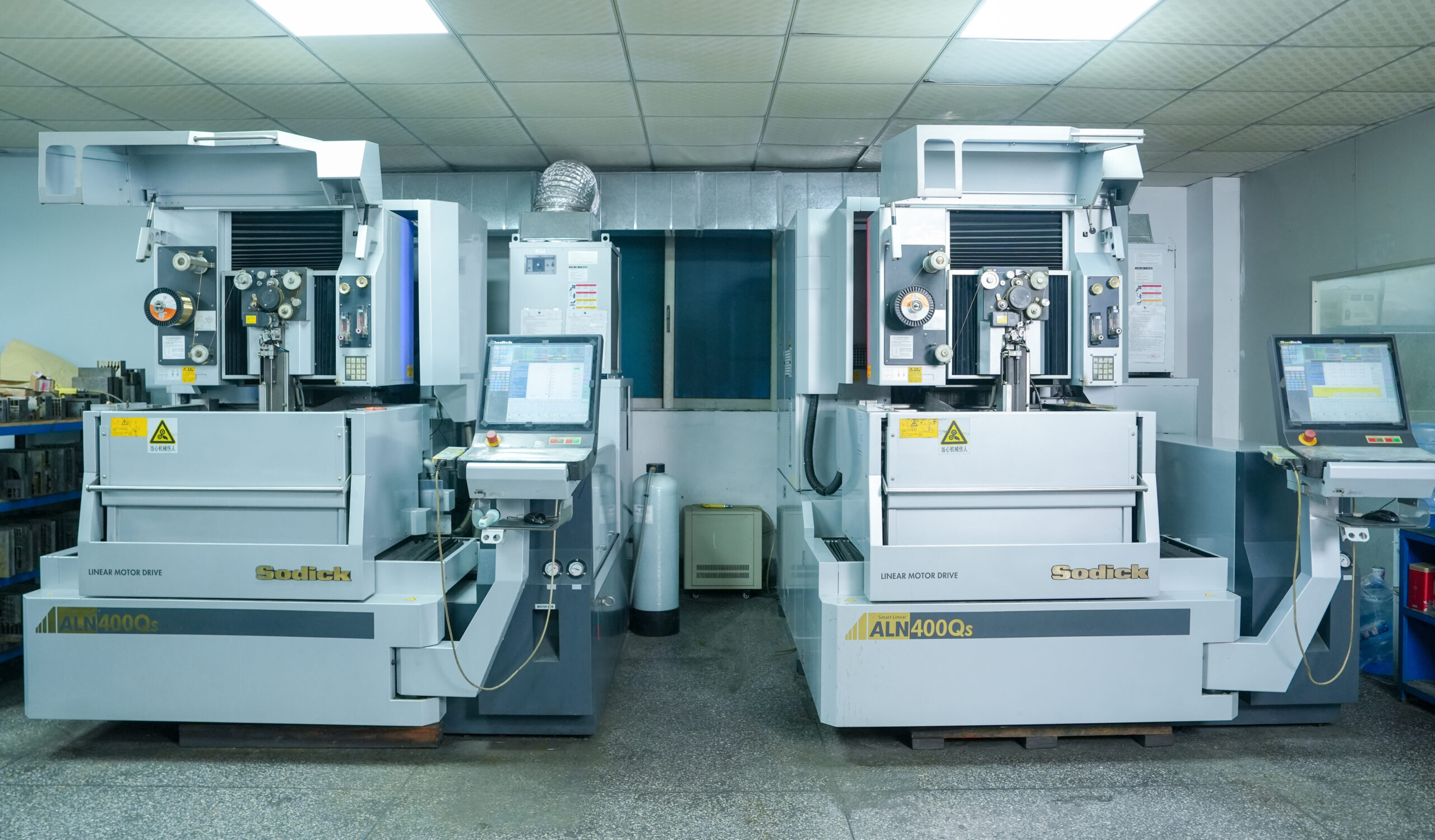
Yicen Precision overcomes these challenges through advanced 5-axis CNC machining that minimizes part handling and ensures geometric accuracy in a single setup. Our climate-controlled manufacturing environment maintains consistent temperatures within ±1°C, preventing thermal expansion errors. Specialized vacuum fixturing distributes clamping forces evenly, eliminating distortion in thin-walled sections.
We employ precision measurement tools including coordinate measuring machines (CMM) with sub-micron accuracy, laser scanning for flatness verification, and non-contact optical profilometers for surface finish validation. Each wafer handling arm undergoes ultrasonic cleaning and cleanroom packaging to ensure particle-free delivery ready for immediate integration into semiconductor equipment.
D. Aplicações e casos de utilização
Precision-machined wafer handling arms serve critical functions across semiconductor manufacturing:
- EFEM (Equipment Front End Modules) – Automated wafer loading and unloading systems
- Load Port Interfaces – FOUP (Front Opening Unified Pod) to equipment transfer mechanisms
- Atmospheric Transfer Chambers – Wafer transport between ambient and vacuum environments
- Lithography Systems – Precision wafer positioning for photomask alignment
- Inspection Equipment – Wafer handling for defect detection and metrology stations
- Chemical Vapor Deposition (CVD) Tools – High-temperature process chamber loading
- Ion Implantation Systems – Controlled wafer insertion into beam lines
- Wafer Sorters – High-speed automated sorting and binning equipment
E. Why Choose Yicen Precision for Wafer Handling Arms CNC Machining?
Yicen Precision specializes in semiconductor-grade manufacturing with over 15 years of experience producing ultra-precision components for cleanroom applications. Our dedicated semiconductor division understands the critical nature of wafer handling arms and maintains controlled environments throughout the production process. We offer rapid prototyping with 5-7 day lead times for sample parts, scaling seamlessly to high-volume production runs with consistent quality.
Our engineering team provides comprehensive DFM (Design for Manufacturability) consultation, optimizing designs for both performance and cost-effectiveness. Full material traceability with certifications ensures compliance with semiconductor industry standards. We maintain complete documentation packages including dimensional reports, material certificates, and surface cleanliness data.
With competitive pricing structures and flexible MOQs, Yicen Precision delivers wafer handling arms that meet your exact specifications without compromising on the precision and cleanliness your semiconductor processes demand. Contact our technical team for a detailed quote and engineering review.

