1. Startseite
  2. »
  3. Industry
  4. »
  5. Aerospace Industry

Reticle & Mask Housings CNC Machining for Semiconductor Industry

Deliver flawless photolithography performance with ultra-precision reticle and mask housings machined to sub-micron specifications. Yicen Precision engineers cleanroom-compatible carriers and protective housings with exceptional flatness, dimensional stability, and contamination-free surfaces. Ensure pattern integrity and defect-free wafer exposure with our semiconductor-grade manufacturing expertise.

reticle & mask housings cnc machining for semiconductor industry (3)

Powering the Future of Microchips with Precision

In the semiconductor industry, even the smallest variation can disrupt performance. That’s why leading innovators trust Yicen Precision to deliver components with micro-level accuracy. Our advanced CNC machining capabilities allow us to manufacture ultra-tight tolerance parts that are vital for wafer processing, lithography, and packaging equipment. From prototype development to large-scale production, we ensure every piece meets the exacting demands of a sector where precision is not optional, it’s everything.

reticle & mask housings cnc machining for semiconductor industry (2)

CNC Machining Solutions for Reticle & Mask Housings in Semiconductor Manufacturing

Reticle and mask housings are precision-engineered enclosures that protect and position photomasks during the lithography process, where circuit patterns are transferred onto silicon wafers. These critical components must maintain exact positioning accuracy while shielding expensive reticles from contamination, physical damage, and environmental factors. Yicen Precision’s advanced CNC machining capabilities produce reticle mask housings that meet the exacting standards of deep ultraviolet (DUV) and extreme ultraviolet (EUV) lithography systems.

Our 5-axis milling centers and precision multi-axis lathes machine reticle mask housings from aerospace-grade aluminum alloys, anodized aluminum, stainless steel, and specialized low-expansion materials. Every housing component undergoes stringent flatness verification and dimensional inspection to ensure SEMI standard compliance and ISO Class 1 cleanroom compatibility. With advanced precision tooling and sophisticated CAM programming, we achieve the tight tolerances and complex geometries required for SMIF pods, reticle carriers, pellicle frames, and photomask storage systems used in leading-edge semiconductor fabrication facilities worldwide

CNC Parts We Deliver For Semiconductor Industry

We provide ultra-precise CNC machining solutions for semiconductor manufacturing equipment and devices, ensuring micro-level accuracy and reliability for critical operations

State-of-the-Art Facilities

Equipped with the latest technology and advanced machinery to ensure precise, high-quality manufacturing.
Precision Machining Center

High-accuracy CNC manufacturing with advanced technology and unmatched efficiency.

CNC Production Workshop

Streamlined CNC production using state-of-the-art machinery for consistent quality.

Advanced CNC Manufacturing Hub

Expert fabrication and assembly of intricate CNC components under one roof.

Automated Machining Facility

Fully automated CNC operations delivering fast, precise, and reliable machining.

High-Performance CNC Workshop

Optimized for delivering premium-quality CNC parts with speed and precision.

Integrated CNC Production Plant

End-to-end CNC manufacturing with seamless workflows and superior results.

Semiconductor Materials We Machine

Yicen Precision works with ultra-pure metals, specialty alloys, and cleanroom-compatible plastics to ensure the semiconductor industry achieves unmatched accuracy and contamination-free performance.

semiconductor materials we machine
  • Aluminum Alloys: Al 6061-T6, Al 5083, Al 7075
  • Stainless Steel: SS 304L, SS 316L, 17-4PH
  • Copper & Alloys: OFHC Copper, CuBe (Beryllium Copper)
  • Special Alloys: Invar 36, Kovar
  • Plastics: PEEK, PTFE (Teflon), PVDF, Polycarbonate

Semiconductor Surface Finish Options

In semiconductor manufacturing, cleanliness, conductivity, and precision are everything. Yicen Precision provides finishes that meet strict industry standards for contamination control, electrical performance, and long-term durability in cleanroom environments.

semiconductor surface finish options
  • As Machined 
  • Electropolishing 
  • Anodizing
  • Nickel Plating 
  • Gold Plating 
  • Passivation 
  • Ultra-Fine Polishing / Mirror Finish
  • Chemical Vapor Polishing 
  • Cleanroom-Compatible Coatings 
  • Diamond-Like Carbon (DLC) Coating

Industries We Serve

Yicen Precision is serving a broad spectrum of industries, covering aerospace, automotive, electronics, medical, and more. We specialize in providing high-quality, reliable parts tailored to meet the unique engineering challenges of each industry.

What Clients Say

See why clients rely on Yicen Precision for CNC machining. Our testimonials highlight satisfaction with precision, quality, on-time delivery, and dedicated support, fostering lasting partnerships across industries worldwide.

Connect With Us

Transform Concepts into Precision Parts

We specialize in converting your ideas into high-quality, functional components with unparalleled speed and accuracy. With advanced technology and expert craftsmanship, we create parts that meet the most complex specifications.

Get In Touch With Us!
Prompt response guaranteed within 12 hours
🔐 All uploads are secure and confidential

Precision CNC Machining for Reticle & Mask Housings

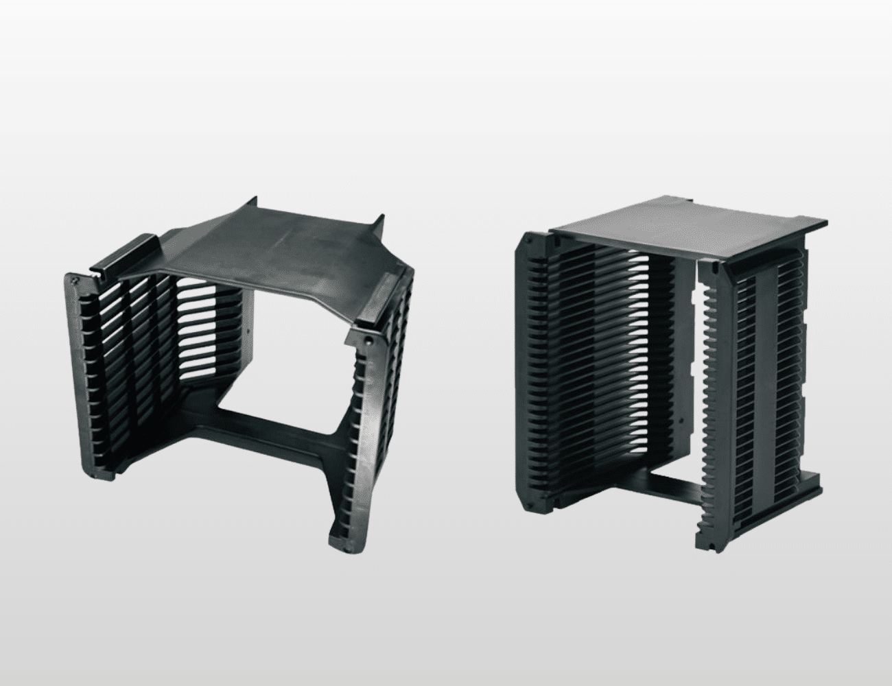
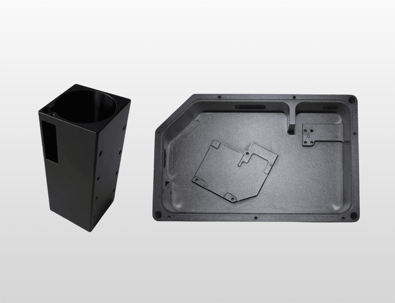
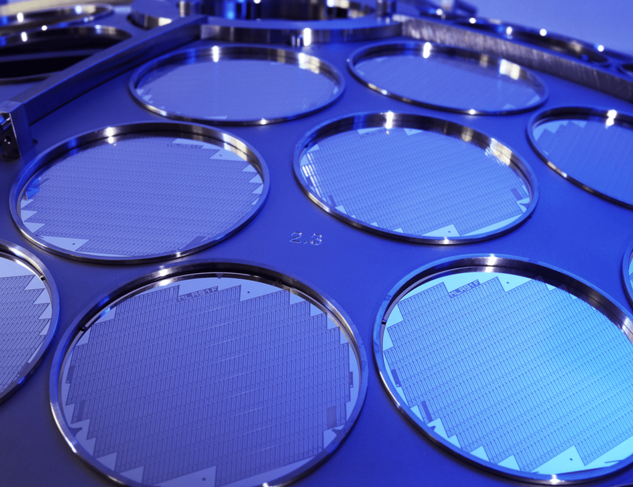
A. What are Reticle & Mask Housings? 

Reticle and mask housings are specialized protective enclosures and positioning systems designed to secure photomasks (reticles) used in semiconductor lithography equipment. These precision-machined components provide contamination barriers while maintaining exact alignment and flatness specifications critical for pattern transfer accuracy. Reticle housings include SMIF (Standard Mechanical Interface) pods, reticle carriers, mask pellicle frames, and storage containers that transport and protect photomasks valued at $50,000-$500,000 each. Operating in Class 1 cleanroom environments, these housings prevent particle contamination, electrostatic discharge, and mechanical damage while ensuring repeatable positioning accuracy within nanometer-level specifications across 200mm and 300mm wafer production lithography systems.

B. Key Technical Requirements

Reticle mask housings CNC machining requires exceptional dimensional control with tolerances typically maintained at ±0.0003″ (±0.0076mm) for critical locating features and mounting surfaces. Flatness specifications for reticle contact surfaces demand deviations less than 0.0005″ across the entire plane to prevent pattern distortion during exposure. Surface finish requirements specify Ra values below 16 microinches (0.4 μm) with mirror-quality finishes on optical pathway surfaces.

Materials must exhibit minimal thermal expansion coefficients (CTE) to maintain dimensional stability across temperature variations in lithography tool environments. Anodized coatings must achieve Class II specifications (0.0002″-0.001″ thickness) for corrosion resistance and wear protection. Perpendicularity and parallelism tolerances often require 0.0002″ or better for kinematic mounting interfaces. ESD-safe materials or coatings are mandatory, with surface resistivity between 10⁶-10⁹ ohms per square. Outgassing properties must meet ASTM E595 standards for vacuum-compatible lithography systems.

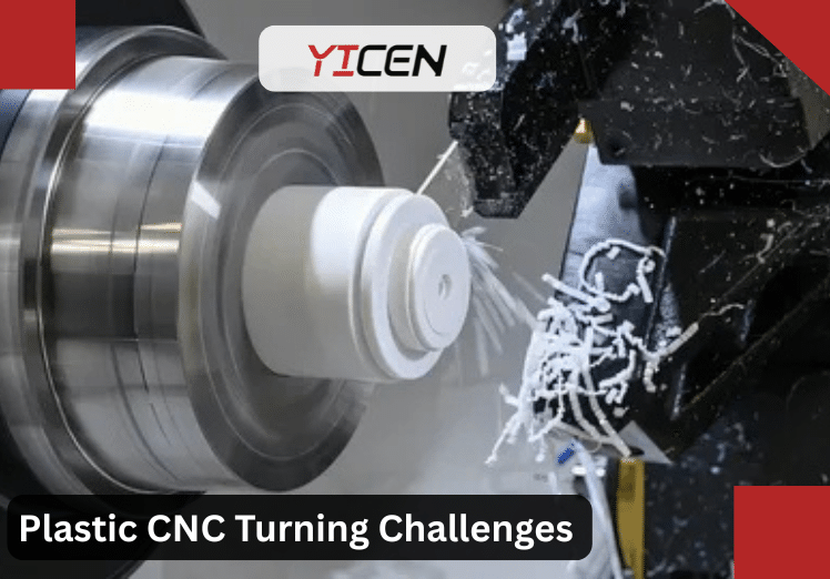
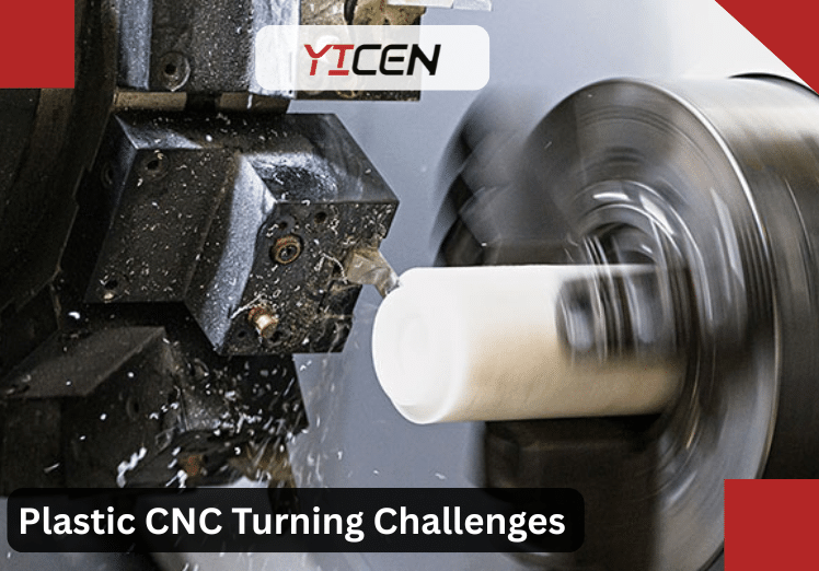
C. Manufacturing Challenges & Solutions

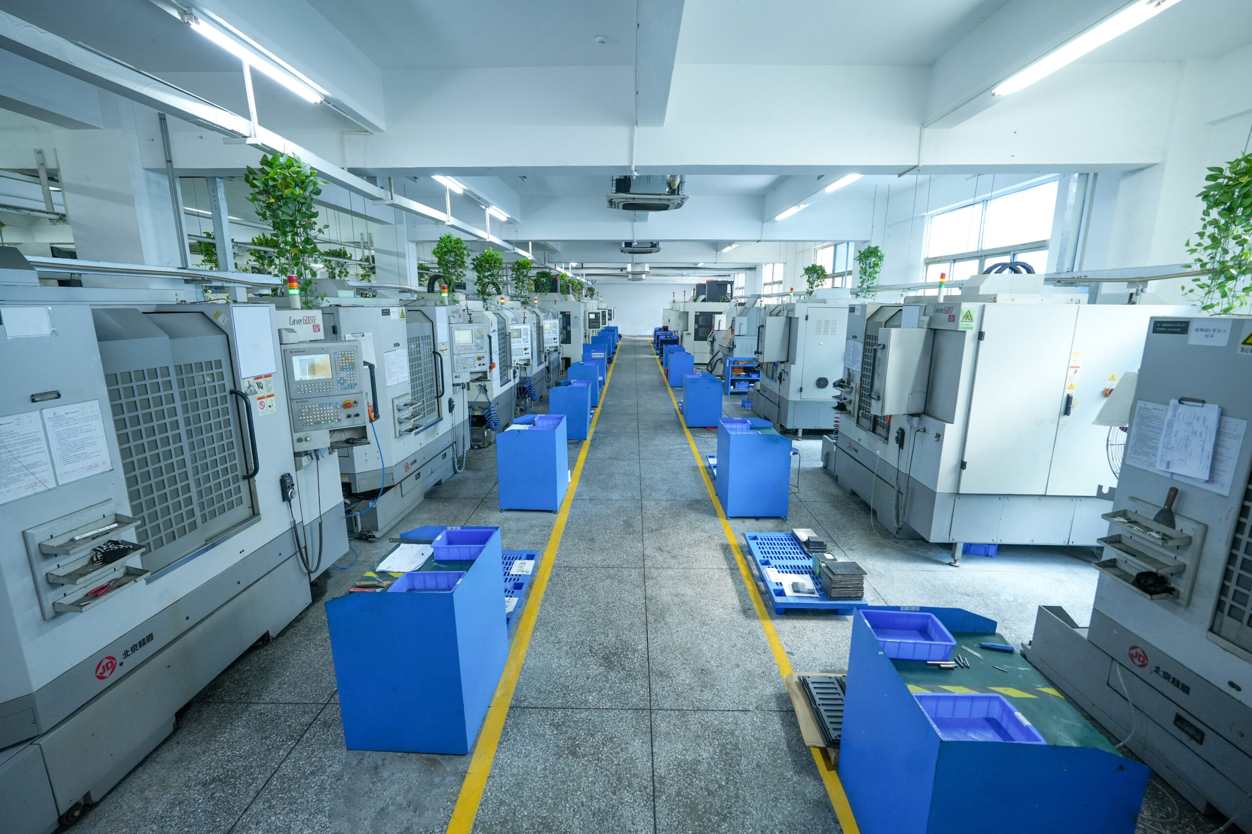
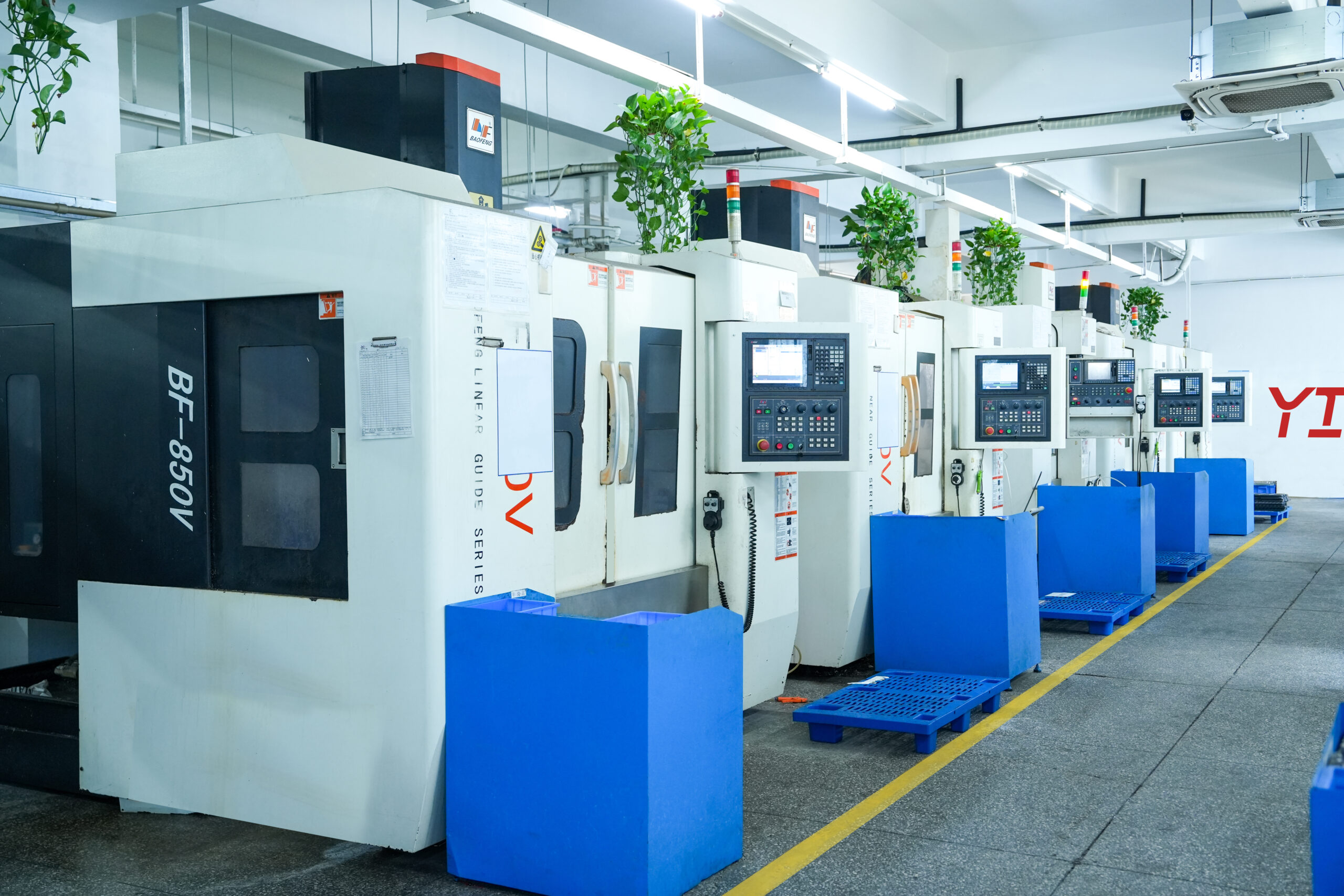
Machining reticle mask housings presents significant challenges due to their complex geometries combining precision pockets, mounting interfaces, and sealing surfaces that must maintain tight tolerances across multiple features simultaneously. Large frame dimensions with thin wall sections are susceptible to machining-induced stress and thermal distortion. Achieving mirror-finish surfaces on aluminum while maintaining dimensional accuracy requires specialized cutting strategies and rigorous process control.

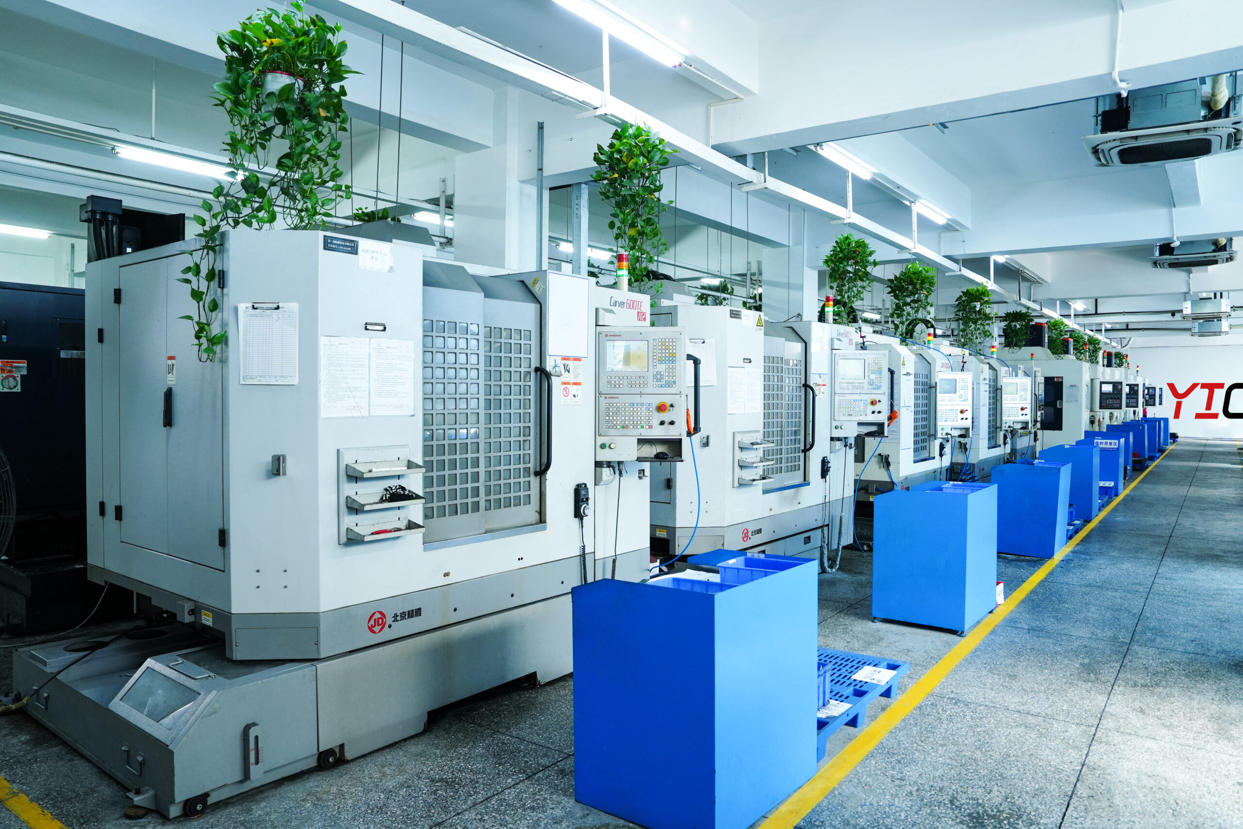
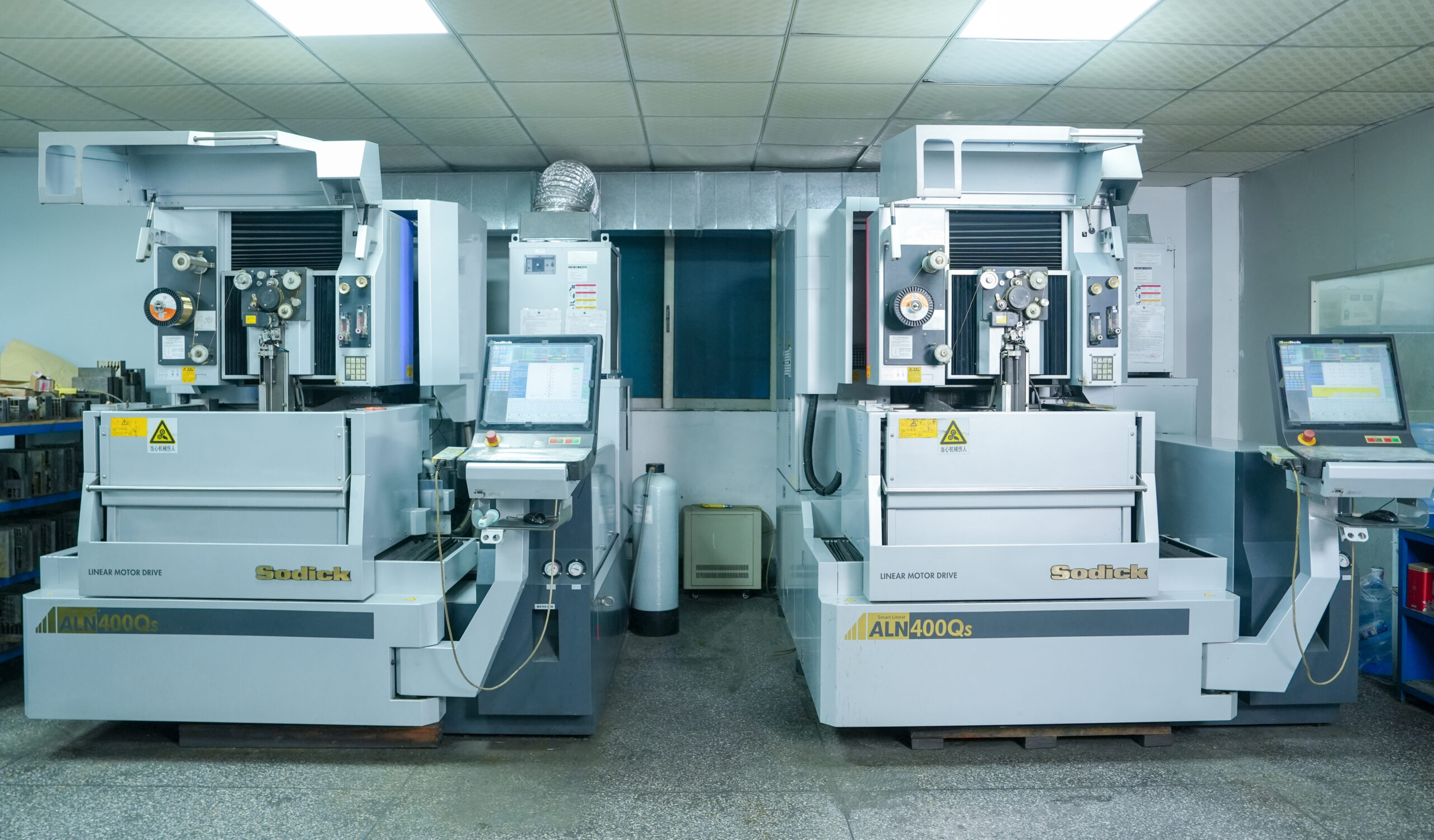
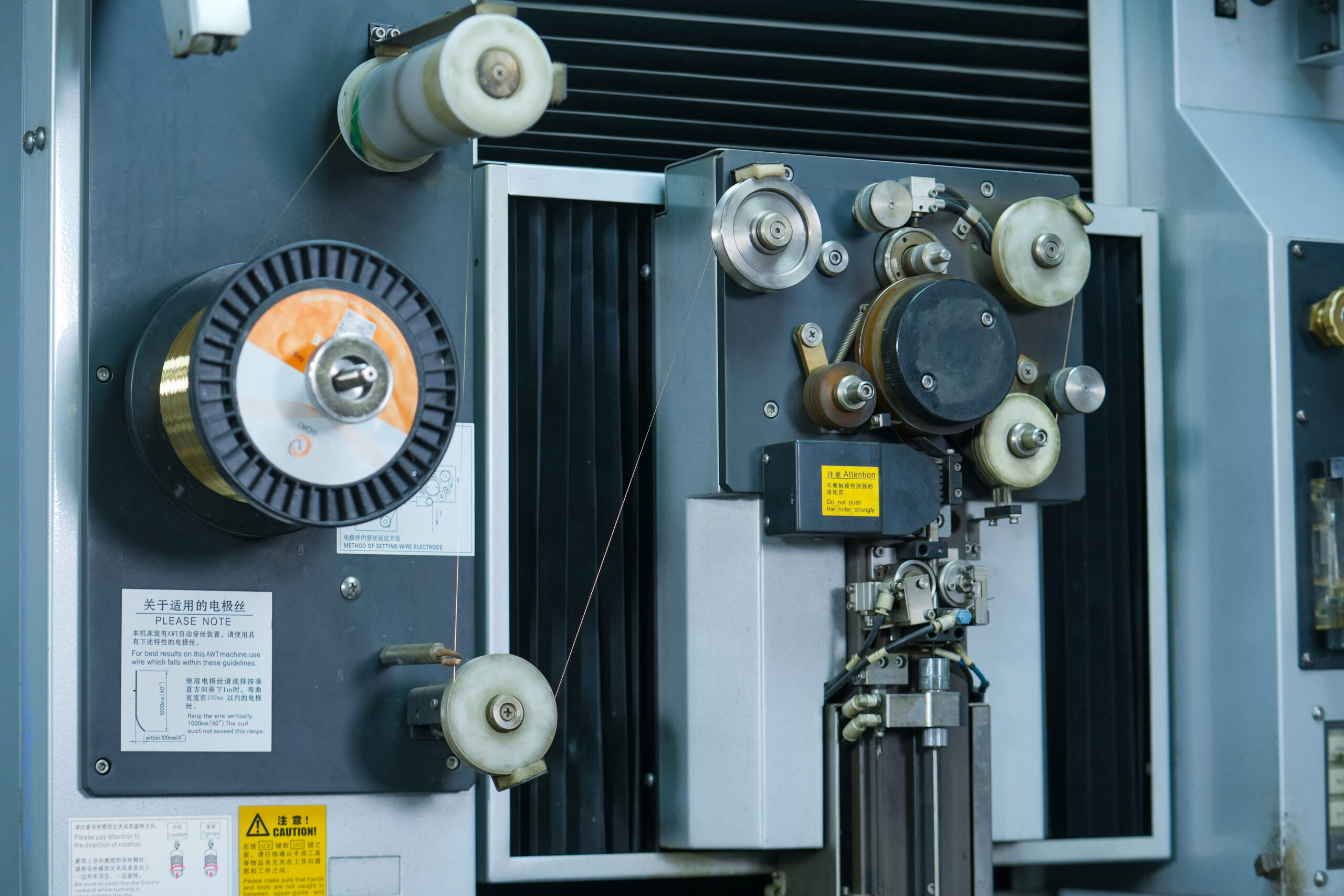
Yicen Precision addresses these challenges through strategic process planning that sequences operations to minimize cumulative errors and residual stresses. Our 5-axis CNC machining centers execute complete operations in single setups, eliminating repositioning errors that could compromise critical dimensions. Temperature-stabilized manufacturing cells maintain ±0.5°C consistency, preventing thermal drift during extended machining cycles.

We utilize diamond-coated carbide tooling and high-speed machining parameters optimized for aluminum and stainless steel, achieving superior surface finishes without secondary operations. Precision fixturing systems incorporate strain-relief designs that support thin-walled sections without inducing deformation. Comprehensive CMM inspection protocols verify all critical dimensions, flatness, and geometric tolerances using sub-micron resolution measurement equipment. Post-machining stress-relief treatments and controlled anodizing processes ensure long-term dimensional stability and surface protection.

D. Applications & Use Cases 

Precision-machined reticle and mask housings serve essential functions across semiconductor lithography operations:

  • SMIF Pods (Standard Mechanical Interface) – Contamination-controlled reticle transport and storage systems
  • Reticle Carriers & Stages – Precision positioning platforms for DUV and EUV lithography scanners
  • Pellicle Frame Assemblies – Protective membrane mounting systems preventing particle defects
  • Photomask Storage Containers – Climate-controlled storage housings for reticle libraries
  • Reticle Inspection Systems – Alignment and defect detection equipment housings
  • Load Port Mechanisms – Automated reticle loading interfaces for steppers and scanners
  • Reticle Handling Robots – End effector mounting systems for automated material handling
  • Calibration Standards Holders – Precision reference reticle positioning fixtures

E. Why Choose Yicen Precision for Reticle & Mask Housings CNC Machining? 

Yicen Precision brings specialized expertise in semiconductor lithography component manufacturing with proven experience producing reticle mask housings for leading equipment manufacturers and fab operators. Our quality management system maintains AS9100 and ISO 9001 certifications with stringent process controls specifically adapted for semiconductor cleanroom applications. We offer rapid prototyping capabilities with 7-10 day turnaround for engineering samples, supporting your development timelines and design validation requirements.

Our materials engineering team provides expert consultation on optimal alloy selection, anodizing specifications, and coating options tailored to your lithography system requirements. Complete material traceability documentation accompanies every shipment, including mill certificates, dimensional inspection reports, and surface finish verification data. We support both low-volume custom projects and high-volume production runs with consistent quality and competitive pricing.

With dedicated project management and engineering support, Yicen Precision ensures your reticle mask housings meet exact specifications for dimensional accuracy, cleanliness, and performance. Request a technical consultation today.

Insights & Articles

Explore Machining services blog for expert insights on CNC machining, industry trends, manufacturing tips, and technology updates—designed to keep you informed, inspired, and ahead in precision engineering.

Frequently Asked Questions

Reticle & Mask Housings

  • What is your typical lead time for custom reticle housing projects?

    Lead times for reticle mask housings depend on design complexity, material selection, and order quantity. Prototype quantities (1-5 pieces) with standard aluminum construction typically ship within 7-10 business days after design approval. Small production runs (10-25 pieces) require approximately 3-4 weeks including machining, anodizing, and inspection. Larger production orders (50+ pieces) are scheduled at 4-6 weeks to accommodate material procurement, manufacturing, and comprehensive quality documentation. For projects requiring specialized materials, coatings, or ultra-precision specifications, we provide detailed timelines during the quotation phase. Expedited services are available for urgent requirements with accelerated scheduling and dedicated manufacturing resources. 

  • How do you ensure particle-free manufacturing for lithography components?

    Particle contamination control is paramount in our reticle mask housing manufacturing process. All final machining operations occur in our Class 1000 cleanroom manufacturing area with HEPA filtration and positive pressure controls. We use dedicated semiconductor-grade cutting fluids and implement comprehensive chip evacuation systems to prevent particle redeposition. Post-machining cleaning includes multi-stage ultrasonic cleaning with semiconductor-grade solvents, DI water rinsing, and nitrogen blow-drying. Parts undergo particle counting verification using light scattering inspection before packaging in double-bagged, ESD-safe cleanroom packaging. Our protocols ensure components arrive ready for immediate integration into Class 1 cleanroom lithography environments. 

  • Can you provide anodized finishes for reticle housings?

    Yes, we offer comprehensive anodizing services specifically calibrated for semiconductor reticle housing applications. Our Type II and Type III hard anodizing processes achieve precise coating thicknesses from 0.0002″ to 0.001″ with excellent uniformity. We provide clear, black, or custom color anodizing with controlled surface resistivity for ESD protection. All anodizing processes are performed to MIL-A-8625 specifications with post-treatment sealing for maximum corrosion resistance. Our quality control includes coating thickness verification, surface resistivity testing, and adhesion testing to ensure long-term durability in cleanroom environments. Material certifications and process documentation are provided with every order.
     

  • What tolerances are achievable for reticle and mask housing components?

    We consistently achieve tolerances of ±0.0003″ (±0.0076mm) for critical mounting surfaces and locating features on reticle mask housings. Flatness specifications are maintained to within 0.0005″ across large frame surfaces, with localized flatness often held to 0.0002″ for reticle contact areas. Perpendicularity and parallelism between critical surfaces routinely meet 0.0002″ tolerances. Our climate-controlled machining environment, precision fixturing, and advanced CMM inspection capabilities ensure these specifications are maintained consistently across production quantities, meeting the demanding requirements of modern lithography equipment manufacturers. 

Get In Touch With Us!
Prompt response guaranteed within 12 hours
🔐 All uploads are secure and confidential