1. Startseite
  2. "
  3. L'industrie
  4. "
  5. Industrie aérospatiale

Wafer Handling Arms CNC Machining for Semiconductor Industry

Achieve ultra-precision wafer handling arms engineered for cleanroom environments with tolerances down to ±0.0005″. Yicen Precision delivers semiconductor-grade CNC machining for automated wafer transfer systems, ensuring contamination-free handling, exceptional repeatability, and zero-defect performance. Request your custom specifications today.

wafer handling arms cnc machining for semiconductor industry

La précision au service de l'avenir des micropuces

Dans l'industrie des semi-conducteurs, la moindre variation peut perturber les performances. C'est pourquoi les principaux innovateurs font confiance à Précision Yicen pour fournir des composants d'une précision de l'ordre du micron. Nos capacités d'usinage CNC avancées nous permettent de fabriquer des pièces à tolérance ultra-serrée qui sont essentielles pour le traitement des plaquettes, la lithographie et l'équipement d'emballage. Du développement de prototypes à la production à grande échelle, nous veillons à ce que chaque pièce réponde aux exigences rigoureuses d'un secteur où la précision n'est pas facultative, mais essentielle.

wafer handling arms cnc machining for semiconductor industry (1)

CNC Machining Solutions for Wafer Handling Arms in Semiconductor

Wafer handling arms are critical components in semiconductor fabrication equipment, responsible for the precise transfer of silicon wafers between processing stations. These components demand exceptional accuracy and contamination-free surfaces to prevent particle generation that could compromise chip yields. Yicen Precision’s advanced CNC machining capabilities deliver wafer handling arms that meet the stringent requirements of cleanroom Class 1-10 environments.

Our state-of-the-art 5-axis milling centers and multi-axis lathes produce wafer handling arms from semiconductor-grade materials including aluminum alloys (6061-T6, 7075), stainless steel (316L), and specialized polymers like PEEK and Delrin. Every component undergoes rigorous dimensional verification and surface cleanliness inspection to ensure compliance with SEMI standards and ISO 9001 protocols. With precision tooling and advanced CAM programming, we achieve the tight tolerances and complex geometries required for robotic wafer handling systems, from EFEM (Equipment Front End Modules) to load ports and atmospheric transfer chambers.

Pièces CNC que nous livrons pour l'industrie des semi-conducteurs

Nous fournissons des solutions d'usinage CNC ultra-précises pour les équipements et dispositifs de fabrication de semi-conducteurs, garantissant une précision et une fiabilité de l'ordre du micro-niveau pour les opérations critiques.

Des installations ultramodernes

Équipés des dernières technologies et de machines de pointe, ils garantissent une fabrication précise et de haute qualité.
Centre d'usinage de précision

Fabrication CNC de haute précision avec une technologie avancée et une efficacité inégalée.

Atelier de production CNC

Rationalisation de la production CNC à l'aide de machines de pointe pour une qualité constante.

Centre de fabrication CNC avancée

Fabrication experte et assemblage de composants CNC complexes sous un même toit.

Installation d'usinage automatisée

Des opérations CNC entièrement automatisées pour un usinage rapide, précis et fiable.

Atelier CNC haute performance

Optimisé pour produire des pièces CNC de qualité supérieure avec rapidité et précision.

Usine de production intégrée à commande numérique

Fabrication CNC de bout en bout avec des flux de travail transparents et des résultats supérieurs.

Machine pour matériaux semi-conducteurs

Yicen Precision travaille avec des métaux ultra-purs, des alliages spéciaux et des plastiques compatibles avec les salles blanches pour garantir à l'industrie des semi-conducteurs une précision inégalée et des performances exemptes de contamination.

matériaux semi-conducteurs que nous traitons
  • Alliages d'aluminium: Al 6061-T6, Al 5083, Al 7075
  • Acier inoxydable: SS 304L, SS 316L, 17-4PH
  • Cuivre et alliages: OFHC Cuivre, CuBe (cuivre béryllium)
  • Alliages spéciaux: Invar 36, Kovar
  • Plastiques: PEEK, PTFE (Téflon), PVDF, Polycarbonate

Options de finition de surface des semi-conducteurs

Dans la fabrication des semi-conducteurs, la propreté, la conductivité et la précision sont essentielles. Yicen Precision propose des finitions qui répondent aux normes industrielles strictes en matière de contrôle de la contamination, de performances électriques et de durabilité à long terme dans les salles blanches.

options de finition de surface des semi-conducteurs
  • Tel qu'usiné 
  • Électropolissage 
  • Anodisation
  • Nickelage 
  • Placage d'or 
  • Passivation 
  • Polissage ultra-fin / Finition miroir
  • Polissage chimique à la vapeur 
  • Revêtements compatibles avec les salles blanches 
  • Revêtement DLC (Diamond-Like Carbon)

Industries que nous servons

Yicen Precision est au service d'un large éventail d'industries, couvrant l'aérospatiale, l'automobile, l'électronique, le médical et bien d'autres encore. Nous sommes spécialisés dans la fourniture de pièces fiables et de haute qualité, conçues pour répondre aux défis techniques uniques de chaque industrie.

Ce que disent les clients

Découvrez pourquoi les clients font confiance à Yicen Precision pour l'usinage CNC. Nos témoignages soulignent la satisfaction que suscitent la précision, la qualité, le respect des délais de livraison et l'assistance dévouée, ce qui favorise des partenariats durables dans des secteurs d'activité du monde entier.

Connectez-vous avec nous

Transformer les concepts en pièces de précision

Nous sommes spécialisés dans la transformation de vos idées en composants fonctionnels de haute qualité, avec une rapidité et une précision inégalées. Grâce à une technologie de pointe et à un savoir-faire expert, nous créons des pièces qui répondent aux spécifications les plus complexes.

Prenez contact avec nous !
Réponse rapide garantie dans les 12 heures
🔐 Tous les téléchargements sont sécurisés et confidentiels

Precision CNC Machining for Wafer Handling Arms

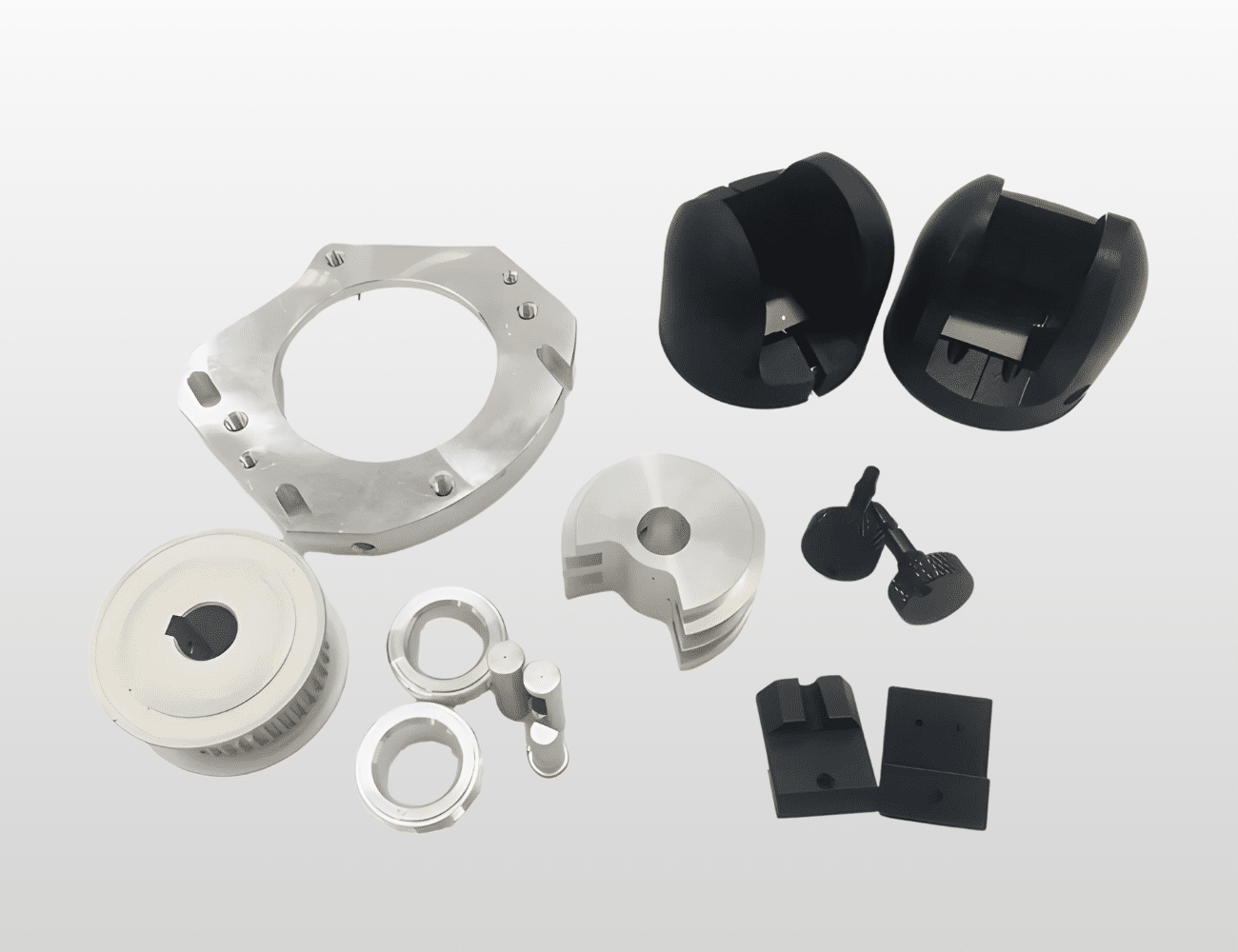
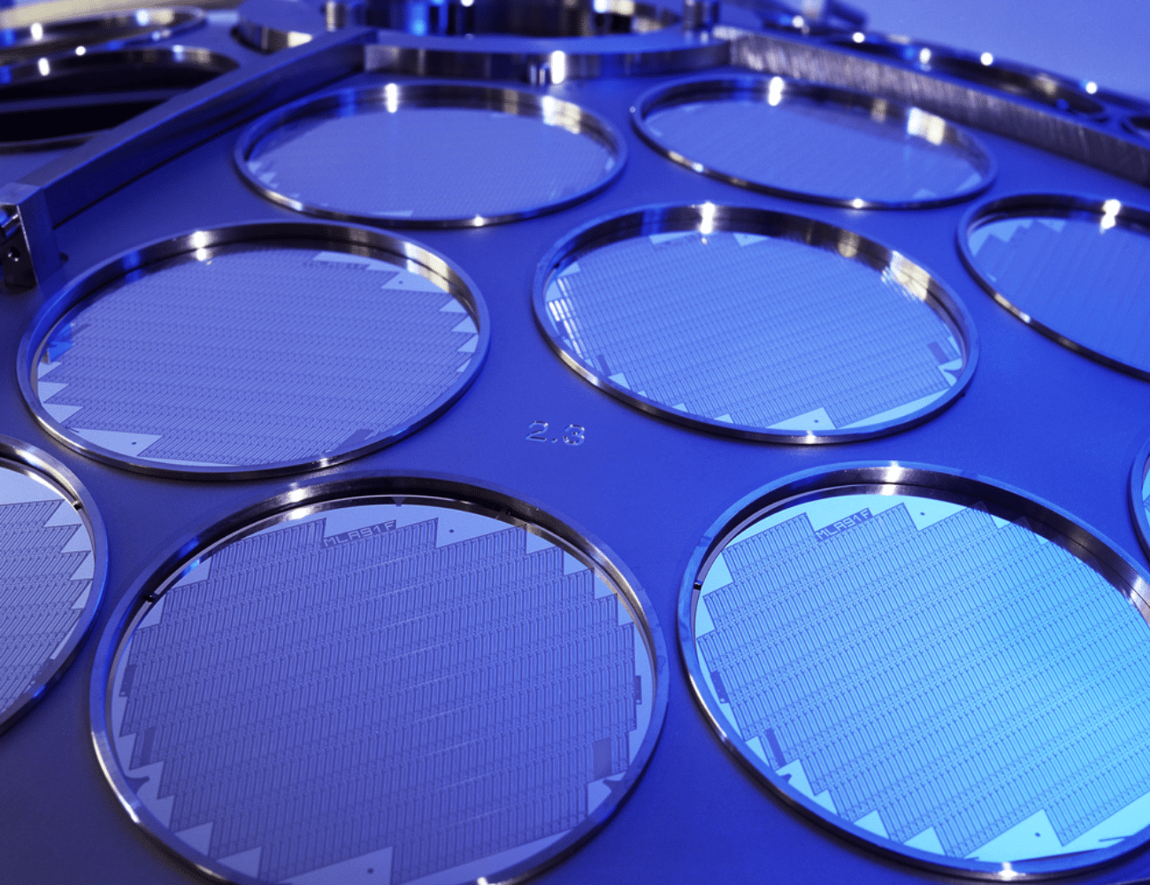
A. What are Wafer Handling Arms? 

Wafer handling arms, also known as end effectors or wafer blades, are robotic components designed to safely grip, transport, and position silicon wafers during semiconductor manufacturing processes. These precision-machined arms operate in ultra-clean environments within automated material handling systems (AMHS), transferring wafers between processing equipment, load ports, and storage cassettes. Critical to maintaining wafer integrity, these arms must provide gentle yet secure handling while generating minimal particles. They are essential in 200mm and 300mm wafer fabs, enabling high-throughput production in applications ranging from lithography and deposition to inspection and testing stations across the semiconductor supply chain.

B. Principales exigences techniques 

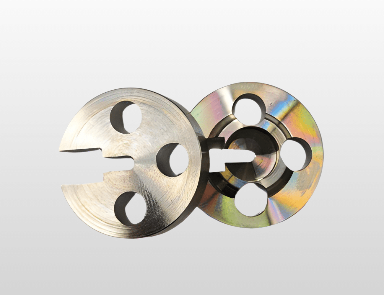
Wafer handling arms CNC machining demands extraordinary precision with tolerances typically held to ±0.0005″ (±0.0127mm) or tighter for critical dimensions. Flatness specifications often require less than 0.001″ across the entire blade surface to prevent wafer warpage or slippage. Surface finish requirements are stringent, with Ra values below 32 microinches (0.8 μm) and often below 16 microinches to minimize particle generation and adhesion points.

Materials must exhibit excellent dimensional stability across temperature fluctuations (typically 20-25°C in fabs), low outgassing properties for vacuum compatibility, and resistance to cleaning chemicals including IPA, acetone, and piranha solutions. Load-bearing capacity must support 300mm wafers (up to 125g) with deflection under 0.1mm at maximum extension. Electrostatic discharge (ESD) protection and non-magnetic properties are often specified for sensitive fabrication environments.

C. Défis et solutions en matière de fabrication 

Machining wafer handling arms presents unique challenges due to their thin, flat geometry prone to distortion during cutting operations. Maintaining flatness while achieving tight tolerances across extended blade lengths requires specialized fixturing and low-stress clamping techniques. Material selection adds complexity—aluminum alloys demand different cutting strategies than engineered polymers, each requiring optimized feeds, speeds, and tool geometries to prevent surface defects or dimensional drift.

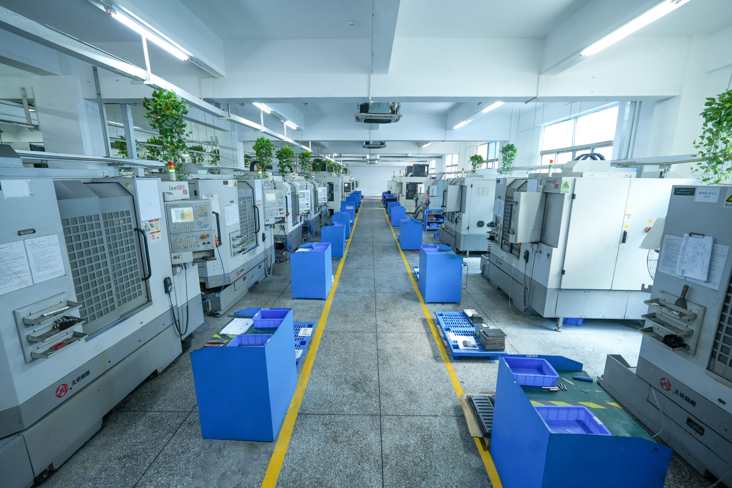
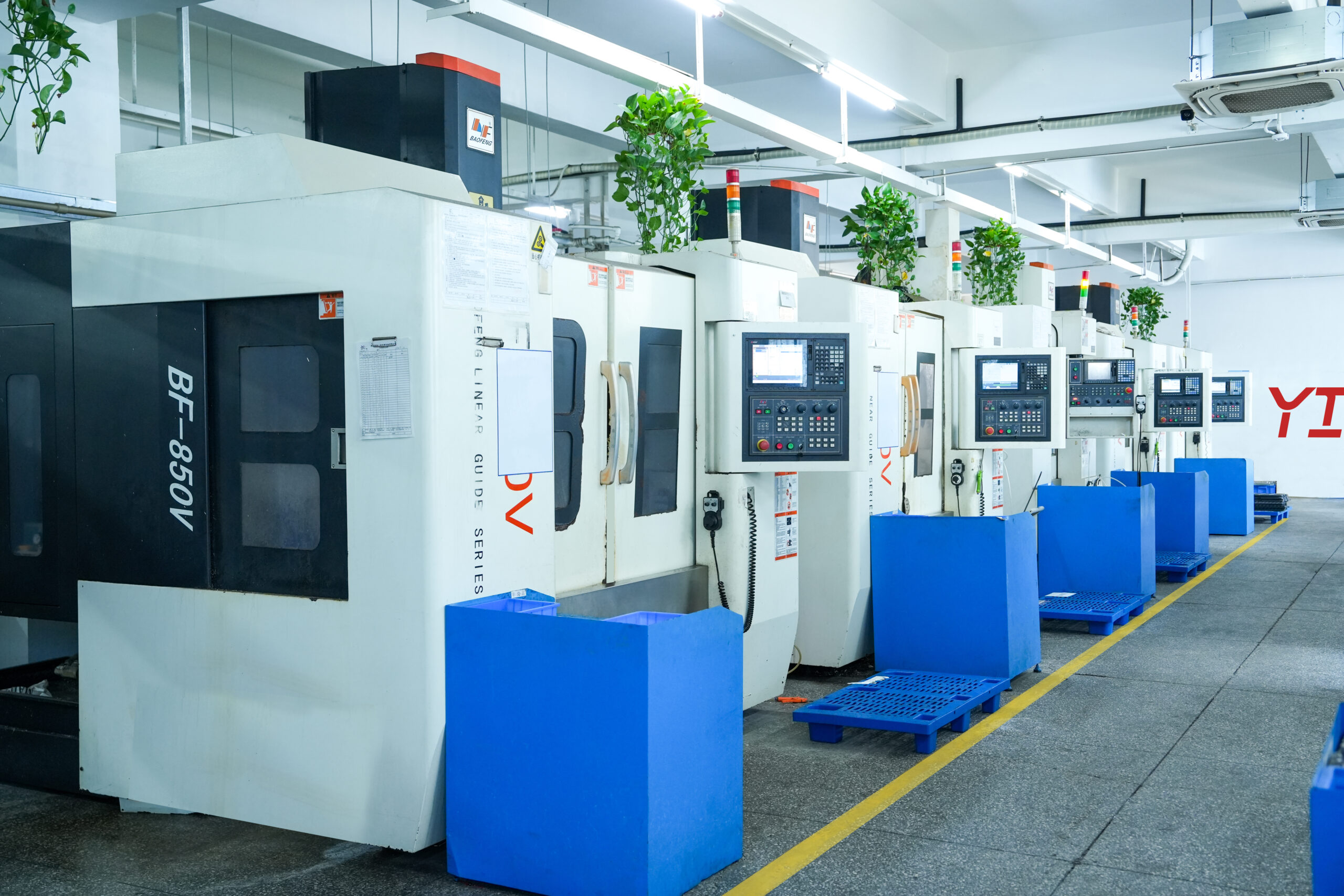
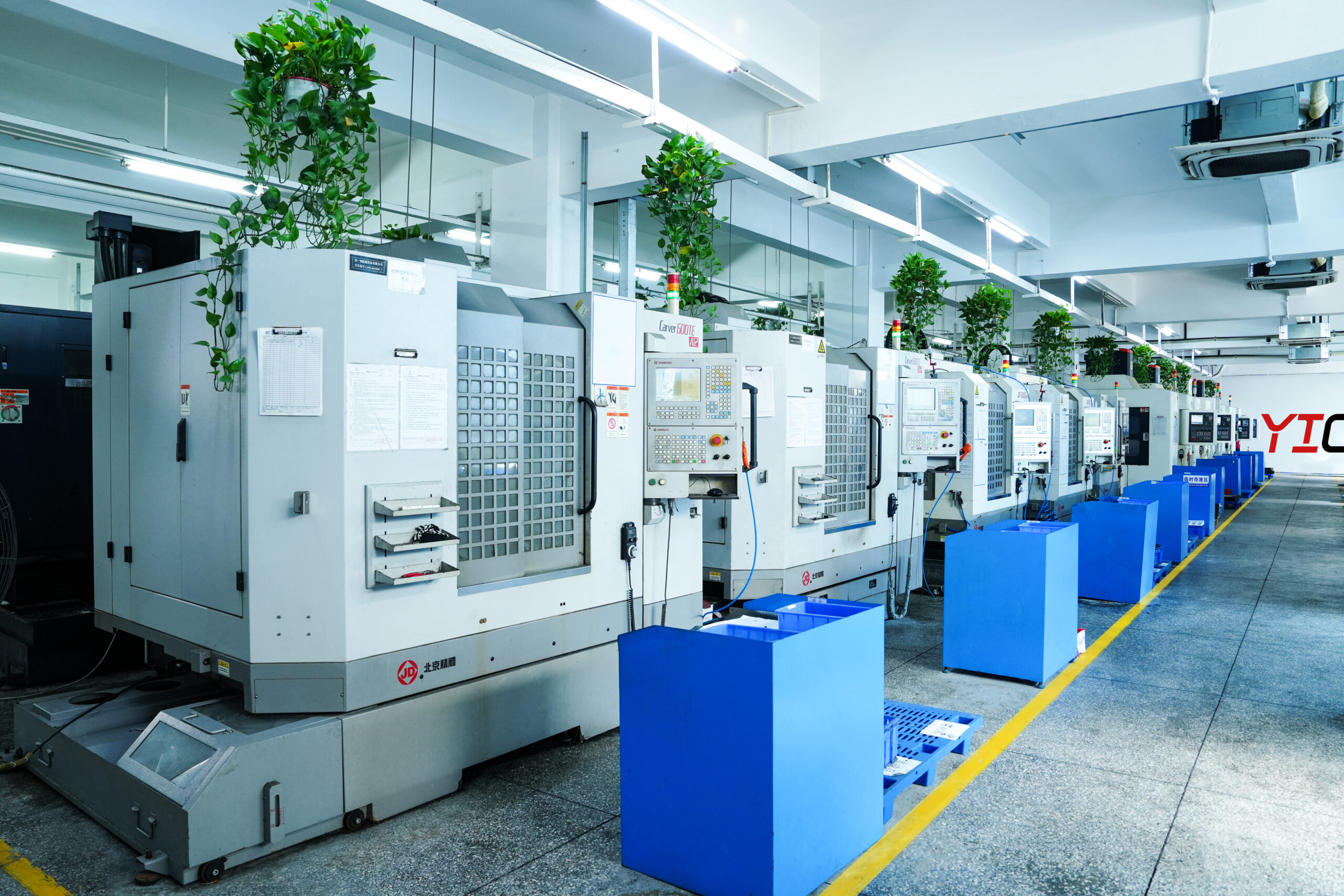
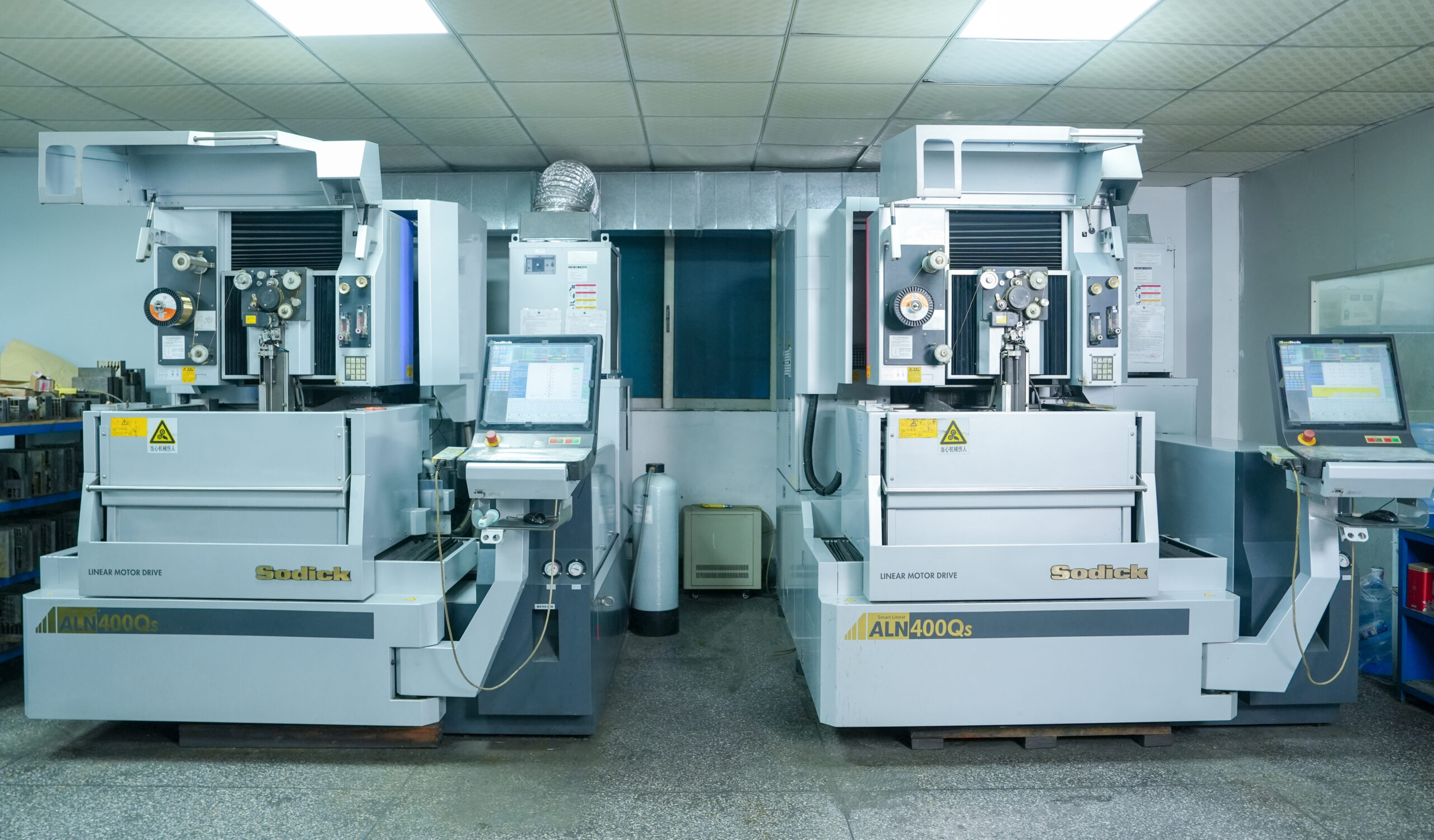
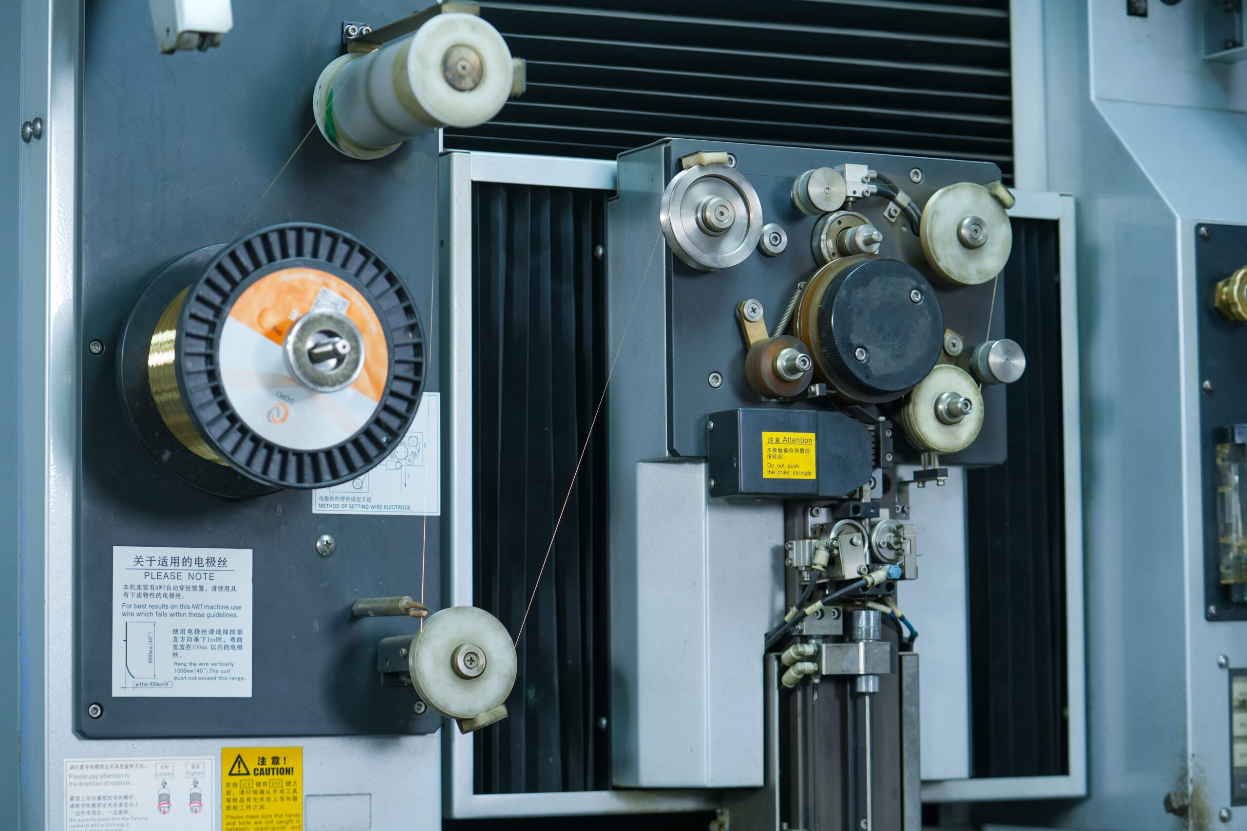
Yicen Precision overcomes these challenges through advanced 5-axis CNC machining that minimizes part handling and ensures geometric accuracy in a single setup. Our climate-controlled manufacturing environment maintains consistent temperatures within ±1°C, preventing thermal expansion errors. Specialized vacuum fixturing distributes clamping forces evenly, eliminating distortion in thin-walled sections.

We employ precision measurement tools including coordinate measuring machines (CMM) with sub-micron accuracy, laser scanning for flatness verification, and non-contact optical profilometers for surface finish validation. Each wafer handling arm undergoes ultrasonic cleaning and cleanroom packaging to ensure particle-free delivery ready for immediate integration into semiconductor equipment.

D. Applications et cas d'utilisation 

Precision-machined wafer handling arms serve critical functions across semiconductor manufacturing:

  • EFEM (Equipment Front End Modules) – Automated wafer loading and unloading systems
  • Load Port Interfaces – FOUP (Front Opening Unified Pod) to equipment transfer mechanisms
  • Atmospheric Transfer Chambers – Wafer transport between ambient and vacuum environments
  • Lithography Systems – Precision wafer positioning for photomask alignment
  • Inspection Equipment – Wafer handling for defect detection and metrology stations
  • Chemical Vapor Deposition (CVD) Tools – High-temperature process chamber loading
  • Ion Implantation Systems – Controlled wafer insertion into beam lines
  • Wafer Sorters – High-speed automated sorting and binning equipment

E. Why Choose Yicen Precision for Wafer Handling Arms CNC Machining? 

Yicen Precision specializes in semiconductor-grade manufacturing with over 15 years of experience producing ultra-precision components for cleanroom applications. Our dedicated semiconductor division understands the critical nature of wafer handling arms and maintains controlled environments throughout the production process. We offer rapid prototyping with 5-7 day lead times for sample parts, scaling seamlessly to high-volume production runs with consistent quality.

Our engineering team provides comprehensive DFM (Design for Manufacturability) consultation, optimizing designs for both performance and cost-effectiveness. Full material traceability with certifications ensures compliance with semiconductor industry standards. We maintain complete documentation packages including dimensional reports, material certificates, and surface cleanliness data.

With competitive pricing structures and flexible MOQs, Yicen Precision delivers wafer handling arms that meet your exact specifications without compromising on the precision and cleanliness your semiconductor processes demand. Contact our technical team for a detailed quote and engineering review.

Perspectives et articles

Explorer Services d'usinage pour obtenir des avis d'experts sur l'usinage CNC, les tendances de l'industrie, les conseils de fabrication et les mises à jour technologiques - conçus pour vous informer, vous inspirer et vous donner une longueur d'avance dans l'ingénierie de précision.

Questions fréquemment posées

Bras de manutention des plaquettes

  • What is the typical lead time for custom wafer handling arms?

    Lead times vary based on complexity and order volume. For prototype and sample quantities (1-10 pieces), we typically deliver within 5-7 business days after design approval. Small production runs (10-50 pieces) require 2-3 weeks, while larger volume orders (100+ pieces) are scheduled at 3-4 weeks. Rush services are available for urgent requirements with expedited machining and inspection. We maintain transparent communication throughout production, providing regular updates and quality documentation with every shipment. Contact us with your specifications for an accurate timeline and competitive quote.
     

  • How do you ensure cleanroom-compatible manufacturing for wafer handling arms?

    All wafer handling arms undergo specialized cleaning and packaging protocols to ensure cleanroom compatibility. After CNC machining, parts are precision-cleaned using ultrasonic cleaning with semiconductor-grade solvents, removing particulates and residual machining oils. We conduct particle count verification and surface cleanliness testing before packaging in cleanroom-certified materials. Our final inspection area maintains Class 100 cleanroom conditions, and all components are double-bagged in antistatic, low-particulate packaging suitable for direct introduction into Class 1-10 cleanroom environments.
     

  • Which materials are best for semiconductor wafer handling arms?

    The optimal material depends on your specific application requirements. Aluminum alloys (6061-T6, 7075-T6) offer excellent strength-to-weight ratios and are widely used for atmospheric handling. Stainless steel 316L provides superior chemical resistance and durability in corrosive environments. For vacuum applications, we recommend engineered polymers like PEEK or Delrin, which offer low outgassing, excellent dimensional stability, and ESD properties. Our engineering team can recommend the best material based on your operating environment, temperature range, and contamination control requirements. 

  • What tolerances can you achieve for wafer handling arms CNC machining?

    We routinely achieve tolerances of ±0.0005″ (±0.0127mm) for critical dimensions on wafer handling arms, with flatness specifications maintained to within 0.001″ across the blade surface. For ultra-precision applications, we can hold tolerances as tight as ±0.0002″ using specialized measurement and process controls. Our climate-controlled machining environment and advanced CMM inspection capabilities ensure consistent dimensional accuracy across production runs, meeting SEMI standards for semiconductor equipment components. 

Prenez contact avec nous !
Réponse rapide garantie dans les 12 heures
🔐 Tous les téléchargements sont sécurisés et confidentiels