


Yicen applies strict inspection, material certification, and finishing standards so that every part performs flawlessly in sensitive semiconductor processes.
 Skip to content
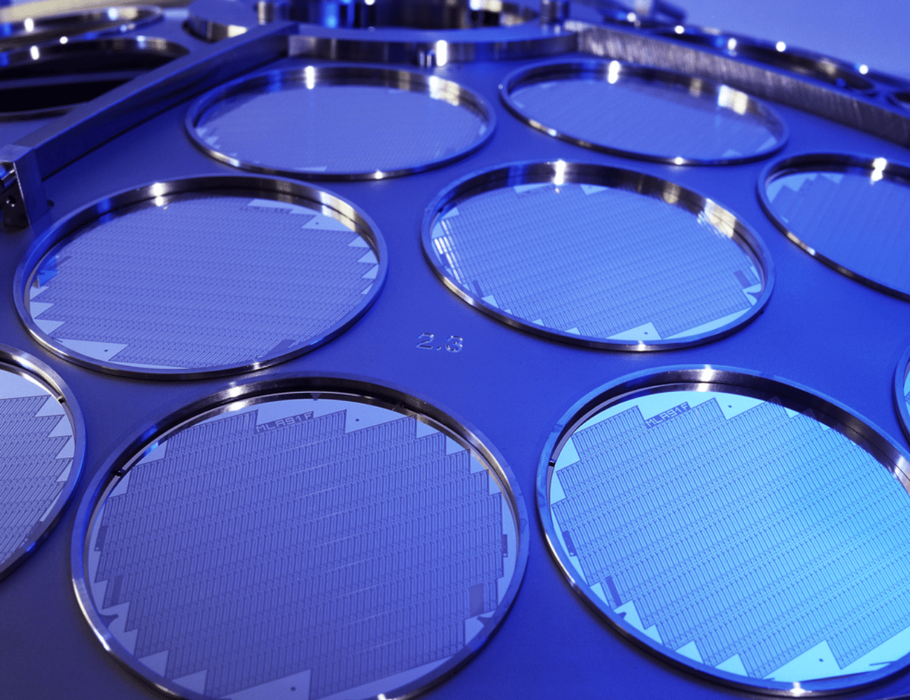
 Precision-machined probe card components engineered for accurate semiconductor wafer testing and high-volume production environments. Our CNC machining delivers exceptional flatness, positional accuracy, and surface quality critical for reliable electrical contact and testing performance. Trust Yicen Precision for probe card components that ensure optimal test yield and measurement accuracy.
In the semiconductor industry, even the smallest variation can disrupt performance. That’s why leading innovators trust Yicen Precision to deliver components with micro-level accuracy. Our advanced CNC machining capabilities allow us to manufacture ultra-tight tolerance parts that are vital for wafer processing, lithography, and packaging equipment. From prototype development to large-scale production, we ensure every piece meets the exacting demands of a sector where precision is not optional, it’s everything.

Probe card components are mission-critical elements in semiconductor wafer testing, requiring extraordinary precision to ensure accurate electrical measurements across thousands of die sites. Yicen Precision specializes in manufacturing high-performance probe card components that meet the demanding requirements of automated test equipment and wafer probe stations. Our expertise ensures every component delivers the dimensional accuracy and surface quality essential for consistent probe contact and reliable test results.
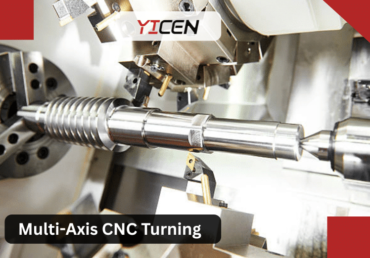
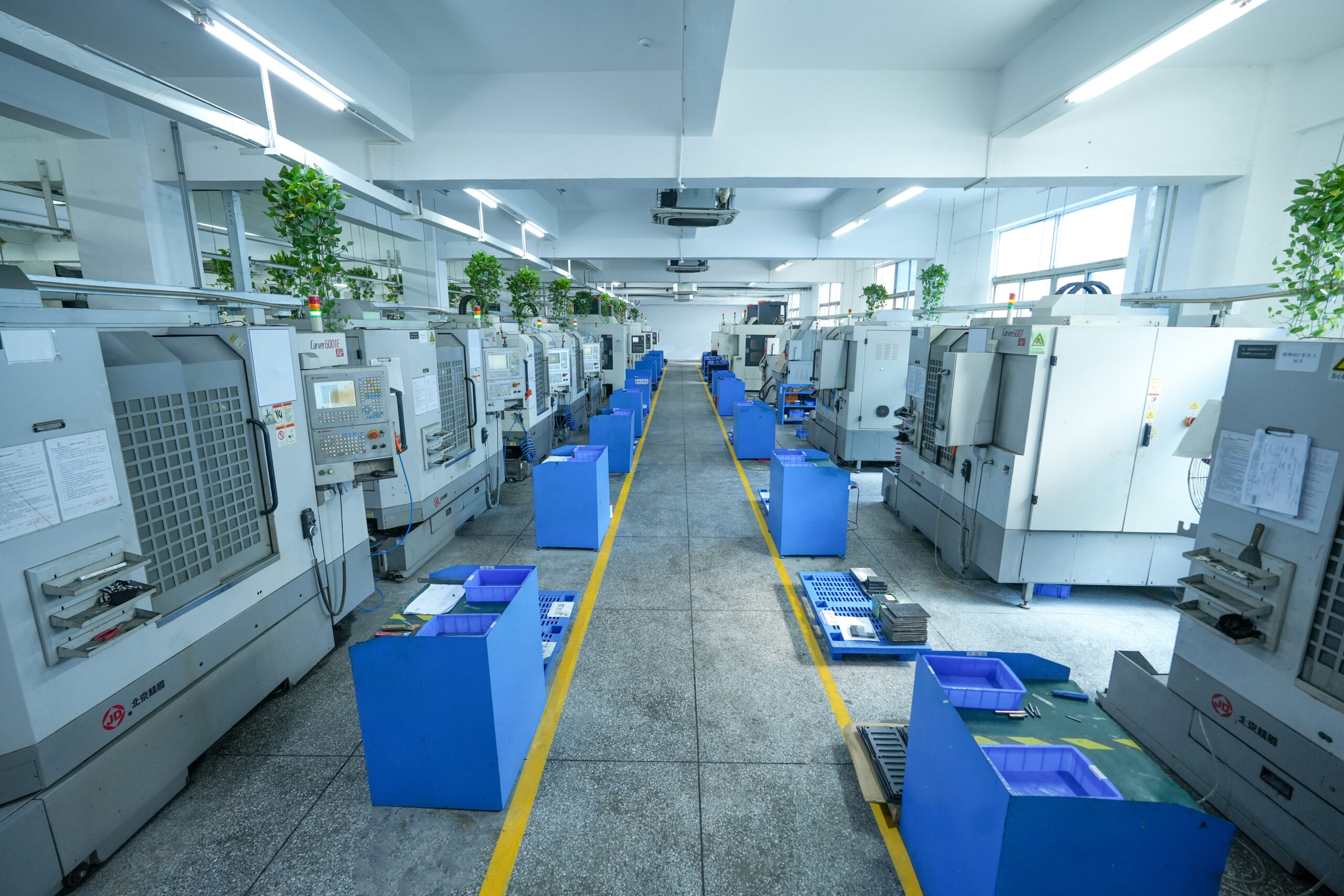
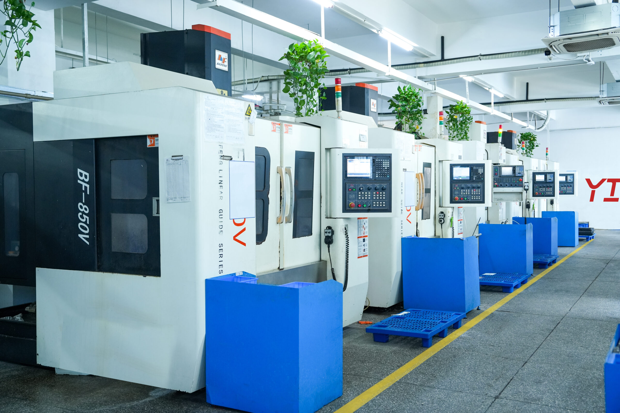
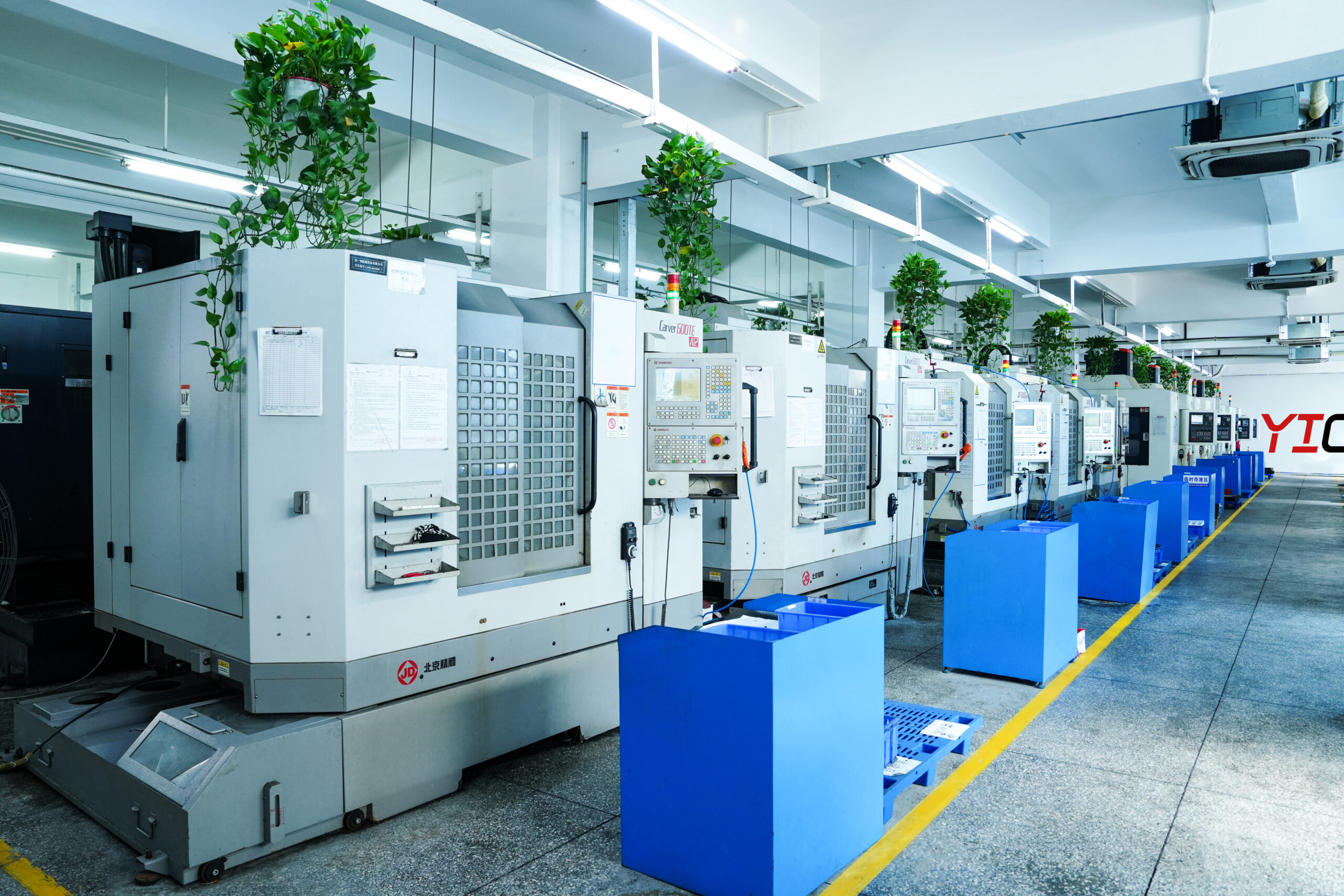
Our advanced CNC machining capabilities, including 5-axis milling and precision grinding operations, enable us to produce complex probe card components with micron-level accuracy. We machine specialized materials such as tungsten carbide, titanium alloys, stainless steel, and ceramic-filled composites using precision tooling designed for ultra-fine tolerances. With ISO 9001 and AS9100 compliance, we deliver probe card components achieving tolerances down to ±0.00005″ while maintaining exceptional flatness specifications critical for uniform probe tip contact across entire wafer surfaces.
We provide ultra-precise CNC machining solutions for semiconductor manufacturing equipment and devices, ensuring micro-level accuracy and reliability for critical operations
High-accuracy CNC manufacturing with advanced technology and unmatched efficiency.
Streamlined CNC production using state-of-the-art machinery for consistent quality.
Expert fabrication and assembly of intricate CNC components under one roof.
Fully automated CNC operations delivering fast, precise, and reliable machining.
Optimized for delivering premium-quality CNC parts with speed and precision.
End-to-end CNC manufacturing with seamless workflows and superior results.
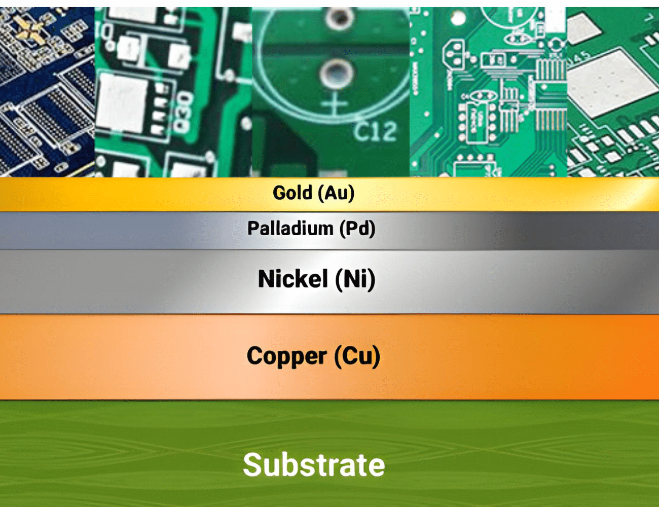
Yicen Precision works with ultra-pure metals, specialty alloys, and cleanroom-compatible plastics to ensure the semiconductor industry achieves unmatched accuracy and contamination-free performance.
In semiconductor manufacturing, cleanliness, conductivity, and precision are everything. Yicen Precision provides finishes that meet strict industry standards for contamination control, electrical performance, and long-term durability in cleanroom environments.
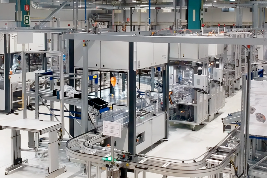
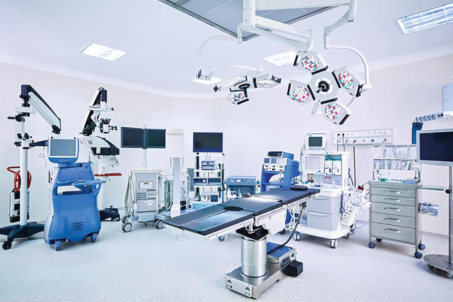
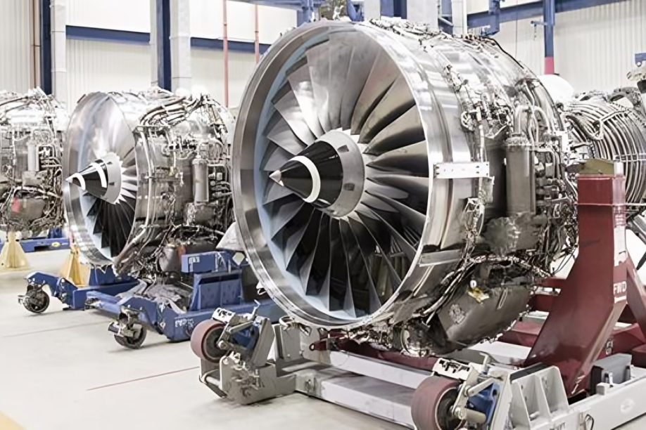
Yicen Precision is serving a broad spectrum of industries, covering aerospace, automotive, electronics, medical, and more. We specialize in providing high-quality, reliable parts tailored to meet the unique engineering challenges of each industry.
See why clients rely on Yicen Precision for CNC machining. Our testimonials highlight satisfaction with precision, quality, on-time delivery, and dedicated support, fostering lasting partnerships across industries worldwide.

Yicen Precision has provided us with top-tier CNC machining services. Their attention to detail and efficiency is unmatched.
Fast turnaround times and precise machining. Yicen Precision always delivers quality work on time, every time.
Outstanding service and reliable machining. Yicen Precision is our go-to supplier for all CNC-related projects.
Great communication and excellent craftsmanship. Yicen Precision consistently meets our demanding specifications.
We specialize in converting your ideas into high-quality, functional components with unparalleled speed and accuracy. With advanced technology and expert craftsmanship, we create parts that meet the most complex specifications.
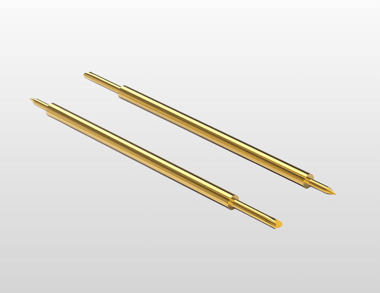
Probe card components are precision-engineered mechanical parts that form the structural framework of probe cards used in semiconductor wafer testing operations. These components include probe card substrates, stiffener rings, mounting plates, guide plates, alignment blocks, and probe tip retention structures that work together to position thousands of electrical probes with micron-level accuracy. Used in wafer sort testing, final test operations, and engineering characterization laboratories, probe card components must deliver exceptional flatness, dimensional stability, and thermal management to ensure reliable electrical contact with semiconductor die pads during high-speed automated testing processes that validate chip functionality before packaging.
Probe card components demand extraordinary precision and material performance characteristics. Positional tolerances of ±0.0001″ or tighter are required for probe tip mounting holes and alignment features to ensure proper electrical contact with microscopic die pads. Flatness specifications typically require 0.0005″ TIR or better across mounting surfaces to maintain uniform probe height and contact force distribution.
Material specifications must provide excellent dimensional stability under thermal cycling from room temperature to 150°C or higher during extended testing operations. Coefficient of thermal expansion matching between substrate materials prevents probe positioning errors during temperature variations. Electrical conductivity or insulation properties depend on component function within the probe card assembly.
Surface finish requirements range from Ra 16-32 microinches for mounting surfaces to Ra 8 microinches or finer for critical datum planes. Parallelism between top and bottom surfaces within 0.0002″ ensures proper mating with test equipment interfaces. Weight optimization reduces inertia for high-speed stepping operations. Corrosion resistance and chemical compatibility with cleaning solvents maintain long-term dimensional accuracy through repeated cleaning cycles.
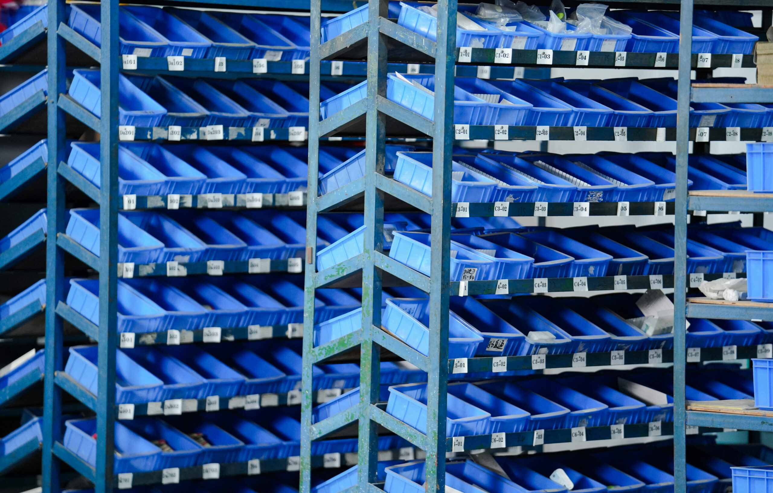
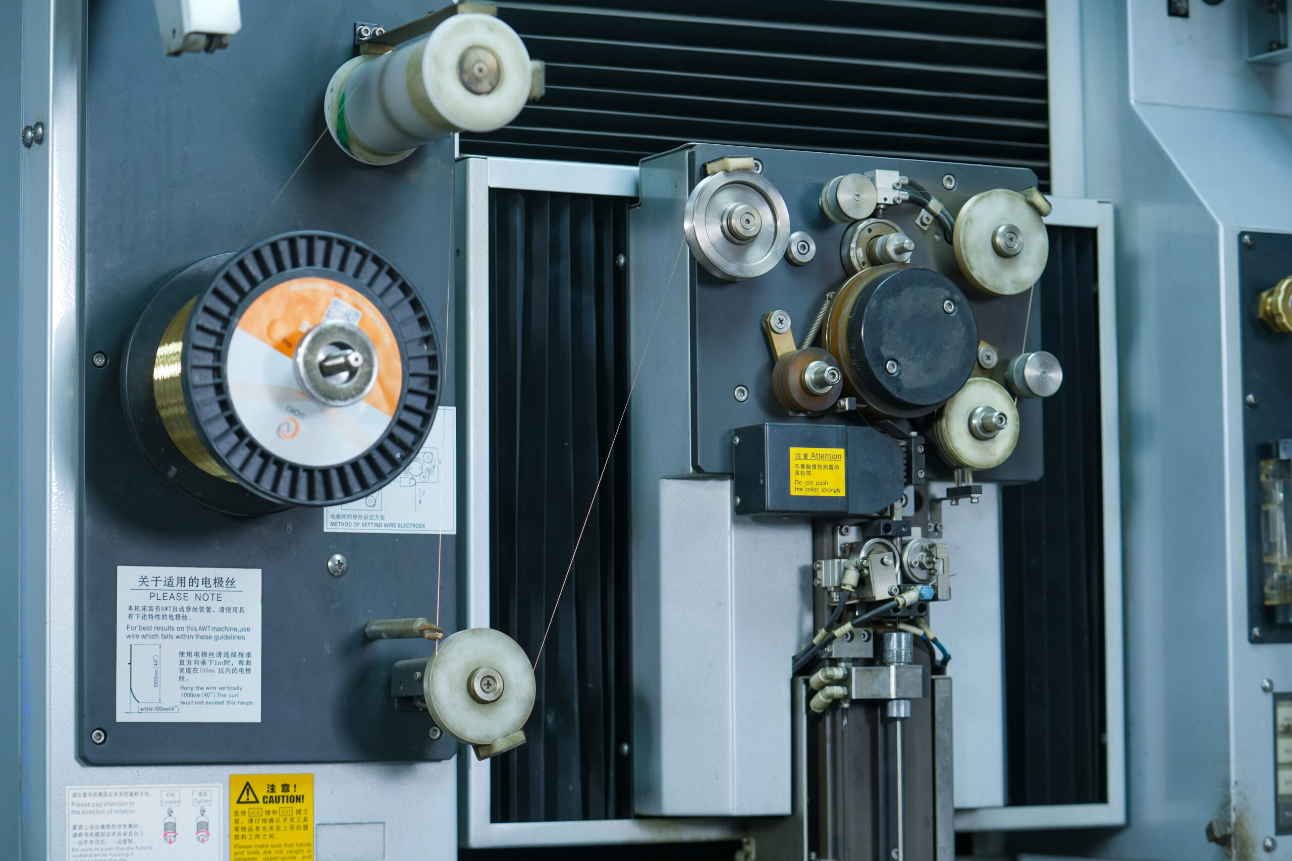
Manufacturing probe card components presents unique challenges including achieving sub-micron flatness across large substrate areas, maintaining precise geometric relationships between thousands of probe mounting holes, and preventing thermal distortion during machining of thin-walled structures. Material challenges include machining tungsten carbide and other ultra-hard materials while achieving fine surface finishes. Burr-free hole drilling at microscopic diameters requires specialized techniques.
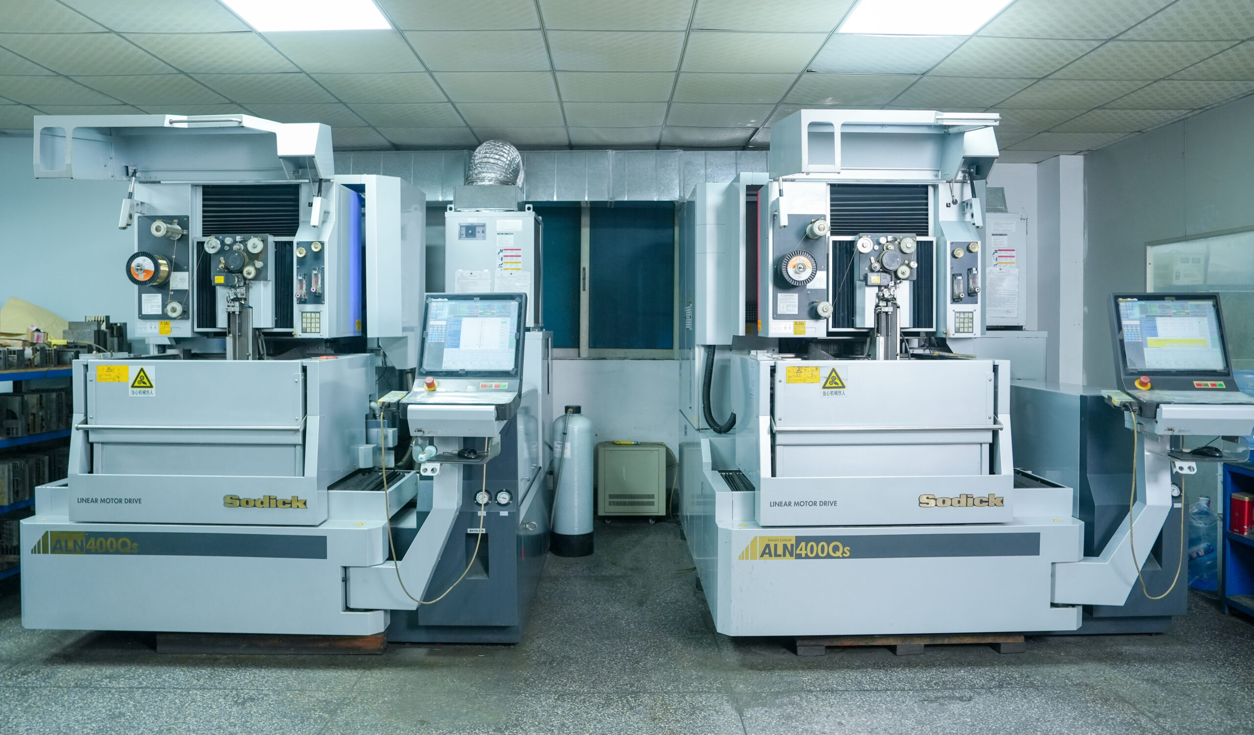
Yicen Precision overcomes these challenges through strategic 5-axis CNC machining combined with precision grinding operations for critical flatness surfaces. Our advanced CAM software optimizes cutting parameters to minimize heat generation and residual stress. Temperature-controlled manufacturing environments prevent thermal drift during precision operations.
We employ specialized carbide tooling and diamond grinding wheels for hard material machining. High-precision drilling techniques with peck cycles and specialized coolant delivery ensure clean, burr-free holes. Stress-relief processes between roughing and finishing operations minimize distortion. Our comprehensive quality control includes CMM inspection with sub-micron resolution, laser interferometry for flatness verification, and optical measurement systems for hole position accuracy. Complete dimensional reports document conformance to exacting probe card specifications.
Precision probe card components manufactured by Yicen Precision serve critical roles across semiconductor testing operations:
Yicen Precision delivers unmatched expertise in semiconductor test tooling and probe card component manufacturing. Our engineering team understands the critical relationships between mechanical precision and electrical test performance. We provide comprehensive DFM consultation to optimize probe card designs for manufacturability, thermal stability, and cost-effectiveness while meeting stringent performance requirements.
Our rapid prototyping capabilities support initial design validation with quick-turn production typically within 1-2 weeks for evaluation samples. Scalability to full production volumes ensures consistent quality from prototype through high-volume manufacturing. Complete material traceability and certification documentation meets semiconductor industry quality standards and supports ongoing reliability analysis.
Cost-effective solutions result from optimized machining strategies, strategic material selection, and design refinement without compromising the micron-level precision and flatness control demanded by modern probe card applications. Our experience across diverse probe card architectures—from traditional cantilever to advanced MEMS and vertical probe technologies—ensures we understand your specific requirements. Contact us for a technical consultation and discover how our probe card component expertise can enhance your test operations.
Explore Machining services blog for expert insights on CNC machining, industry trends, manufacturing tips, and technology updates—designed to keep you informed, inspired, and ahead in precision engineering.
How does Yicen ensure reliability in complex semiconductor assemblies?
Yicen applies strict inspection, material certification, and finishing standards so that every part performs flawlessly in sensitive semiconductor processes.
Are semiconductor CNC parts compatible with automation systems?
CNC-machined parts are built with exact alignment and positioning accuracy, ensuring seamless integration with robotic handling systems used in fabs.
What is the role of CNC in prototyping semiconductor equipment?
CNC machining accelerates R&D by quickly turning design concepts into working prototypes, helping semiconductor companies shorten development cycles.
Can CNC machining reduce contamination risks in cleanrooms?
Yes, CNC parts can be produced with ultra-smooth surfaces and compatible coatings that minimize particle shedding and outgassing, essential for semiconductor cleanrooms.
How does CNC machining support miniaturization in semiconductor devices?
CNC machining allows for micron-level tolerances, making it possible to create ultra-small components that are critical for next-gen semiconductor equipment and devices.