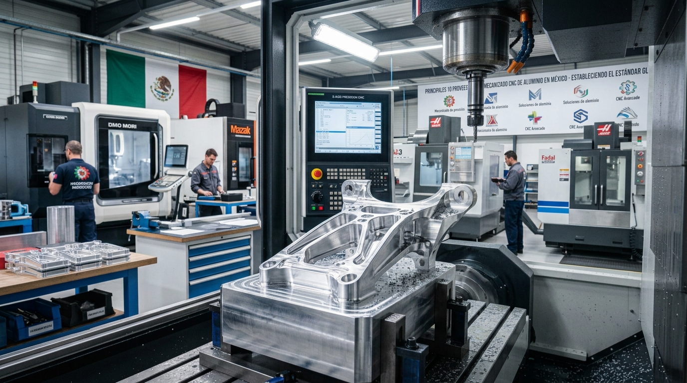
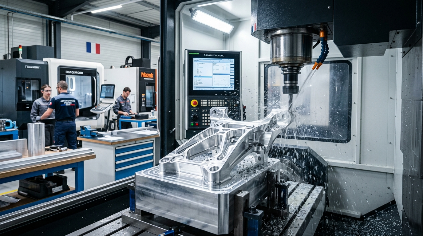
In the semiconductor industry, even the smallest variation can disrupt performance. That’s why leading innovators trust Yicen Precision to deliver components with micro-level accuracy. Our advanced CNC machining capabilities allow us to manufacture ultra-tight tolerance parts that are vital for wafer processing, lithography, and packaging equipment. From prototype development to large-scale production, we ensure every piece meets the exacting demands of a sector where precision is not optional, it’s everything.
Reliable Optical Lens Housings CNC Machining for Semiconductor Applications
Optical lens housings are critical mechanical components in semiconductor manufacturing equipment, requiring precise dimensional control to maintain optical alignment and system performance. Yicen Precision specializes in manufacturing high-precision optical lens housings that meet the demanding requirements of wafer inspection systems, lithography tools, and metrology equipment. Our expertise ensures every housing delivers the bore accuracy and concentricity essential for maintaining optical axis alignment and preventing image aberrations.
Our advanced CNC machining capabilities, including 5-axis milling, precision boring, and multi-axis turning, enable us to produce complex optical lens housings with micron-level accuracy. We machine premium materials such as aluminum 6061-T6, titanium alloys, stainless steel, and brass using precision tooling designed for optical-grade dimensional control. With ISO 9001 and AS9100 compliance, we deliver optical lens housings achieving bore tolerances of ±0.0002″ and concentricity within 0.0005″ TIR, while providing surface treatments including black anodizing and optical blackening critical for stray light suppression in sensitive optical systems.
We provide ultra-precise CNC machining solutions for semiconductor manufacturing equipment and devices, ensuring micro-level accuracy and reliability for critical operations
Equipped with the latest technology and advanced machinery to ensure precise, high-quality manufacturing.
Precision Machining Center
High-accuracy CNC manufacturing with advanced technology and unmatched efficiency.
CNC Production Workshop
Streamlined CNC production using state-of-the-art machinery for consistent quality.
Advanced CNC Manufacturing Hub
Expert fabrication and assembly of intricate CNC components under one roof.
Automated Machining Facility
Fully automated CNC operations delivering fast, precise, and reliable machining.
High-Performance CNC Workshop
Optimized for delivering premium-quality CNC parts with speed and precision.
Integrated CNC Production Plant
End-to-end CNC manufacturing with seamless workflows and superior results.
Semiconductor Materials We Machine
Yicen Precision works with ultra-pure metals, specialty alloys, and cleanroom-compatible plastics to ensure the semiconductor industry achieves unmatched accuracy and contamination-free performance.
In semiconductor manufacturing, cleanliness, conductivity, and precision are everything. Yicen Precision provides finishes that meet strict industry standards for contamination control, electrical performance, and long-term durability in cleanroom environments.
As Machined
Electropolishing
Anodizing
Nickel Plating
Gold Plating
Passivation
Ultra-Fine Polishing / Mirror Finish
Chemical Vapor Polishing
Cleanroom-Compatible Coatings
Diamond-Like Carbon (DLC) Coating
Industries We Serve
Yicen Precision is serving a broad spectrum of industries, covering aerospace, automotive, electronics, medical, and more. We specialize in providing high-quality, reliable parts tailored to meet the unique engineering challenges of each industry.
See why clients rely on Yicen Precision for CNC machining. Our testimonials highlight satisfaction with precision, quality, on-time delivery, and dedicated support, fostering lasting partnerships across industries worldwide.
⭐⭐⭐⭐⭐
Quality You Can Count On
Yicen Precision has provided us with top-tier CNC machining services. Their attention to detail and efficiency is unmatched, ensuring consistent quality and timely delivery across all projects.
John S.
New York, NY
⭐⭐⭐⭐⭐
Fast, Reliable, and Accurate
Fast turnaround times and precise machining. Yicen Precision always delivers quality work on time, every time, with exceptional consistency and reliability.
Sarah T.
Chicago, IL
⭐⭐⭐⭐⭐
Our Go-To CNC Machining Supplier
Outstanding service and reliable machining. Yicen Precision is our go-to supplier for all CNC-related projects, consistently exceeding expectations with quality results.
Michael L.
Seattle, WA
⭐⭐⭐⭐⭐
Reliable, Efficient, and Precise
Great communication and excellent craftsmanship. Yicen Precision consistently meets our demanding specifications, delivering precise results with outstanding consistency.
Emily R.
Austin, TX
Connect With Us
Transform Concepts into Precision Parts
We specialize in converting your ideas into high-quality, functional components with unparalleled speed and accuracy. With advanced technology and expert craftsmanship, we create parts that meet the most complex specifications.
Explore Machining services blog for expert insights on CNC machining, industry trends, manufacturing tips, and technology updates—designed to keep you informed, inspired, and ahead in precision engineering.