A. What are IC Packaging Molds?
IC packaging molds are precision steel tooling systems used in semiconductor packaging operations to encapsulate integrated circuits in protective plastic or epoxy compound materials. These molds consist of cavity blocks, chase assemblies, cull plates, and ejector systems that work together under high temperature and pressure to form consistent package geometries. Used in transfer molding presses, compression molding equipment, and advanced packaging lines, IC packaging molds must deliver exact cavity dimensions, smooth surface finishes, and precise gate configurations to produce defect-free packages across millions of molding cycles while maintaining tight dimensional control for QFN, BGA, SIP, and other package formats.
B. Key Technical Requirements
IC packaging molds demand extraordinary precision and thermal stability. Cavity dimensional tolerances of ±0.0005″ to ±0.001″ are standard to ensure package body dimensions meet specifications. Surface finish requirements are critical, with Ra 4-8 microinches needed for cavity surfaces to facilitate clean part release and prevent surface defects on molded packages.
Material specifications require tool steels with hardness ranging from 28-52 HRC depending on application, providing optimal balance between machinability, wear resistance, and toughness. Thermal stability is essential as molds operate at temperatures between 175-180°C during molding cycles. Materials must maintain dimensional accuracy through thousands of thermal cycles without distortion or cracking.
Flatness and parallelism specifications between parting surfaces within 0.0002″ ensure proper mold closing and prevent flash formation. Gate and runner designs require precise dimensions and smooth transitions to control material flow. Venting channels typically 0.001-0.002″ deep allow trapped air escape without causing flash. Surface treatments including nitriding, PVD coatings, or polishing enhance mold life and release characteristics.
C. Manufacturing Challenges & Solutions
Manufacturing IC packaging molds presents significant challenges including achieving mirror-finish cavity surfaces without tool marks or surface defects, machining complex package geometries with undercuts and fine features, and maintaining precise dimensional relationships between multiple cavities in multi-cavity molds. Material hardness after heat treatment complicates finishing operations. Thermal stability during machining prevents distortion that would compromise cavity accuracy.
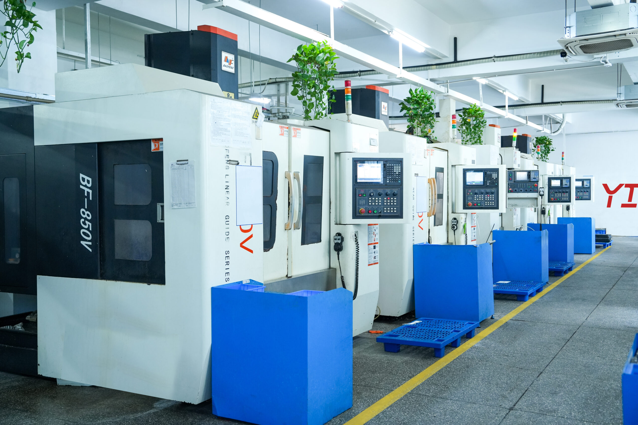
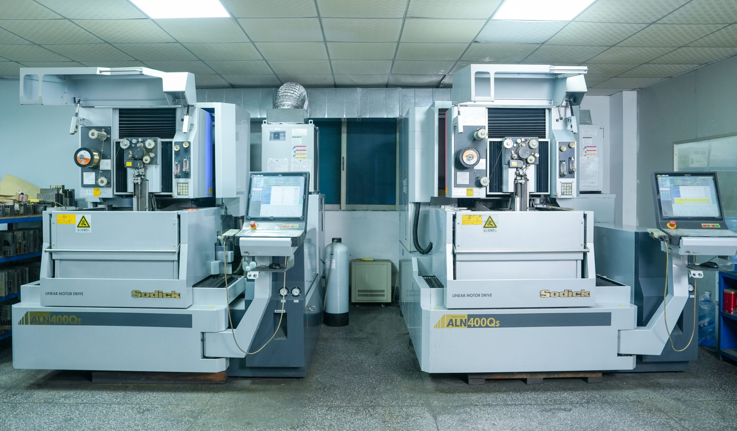
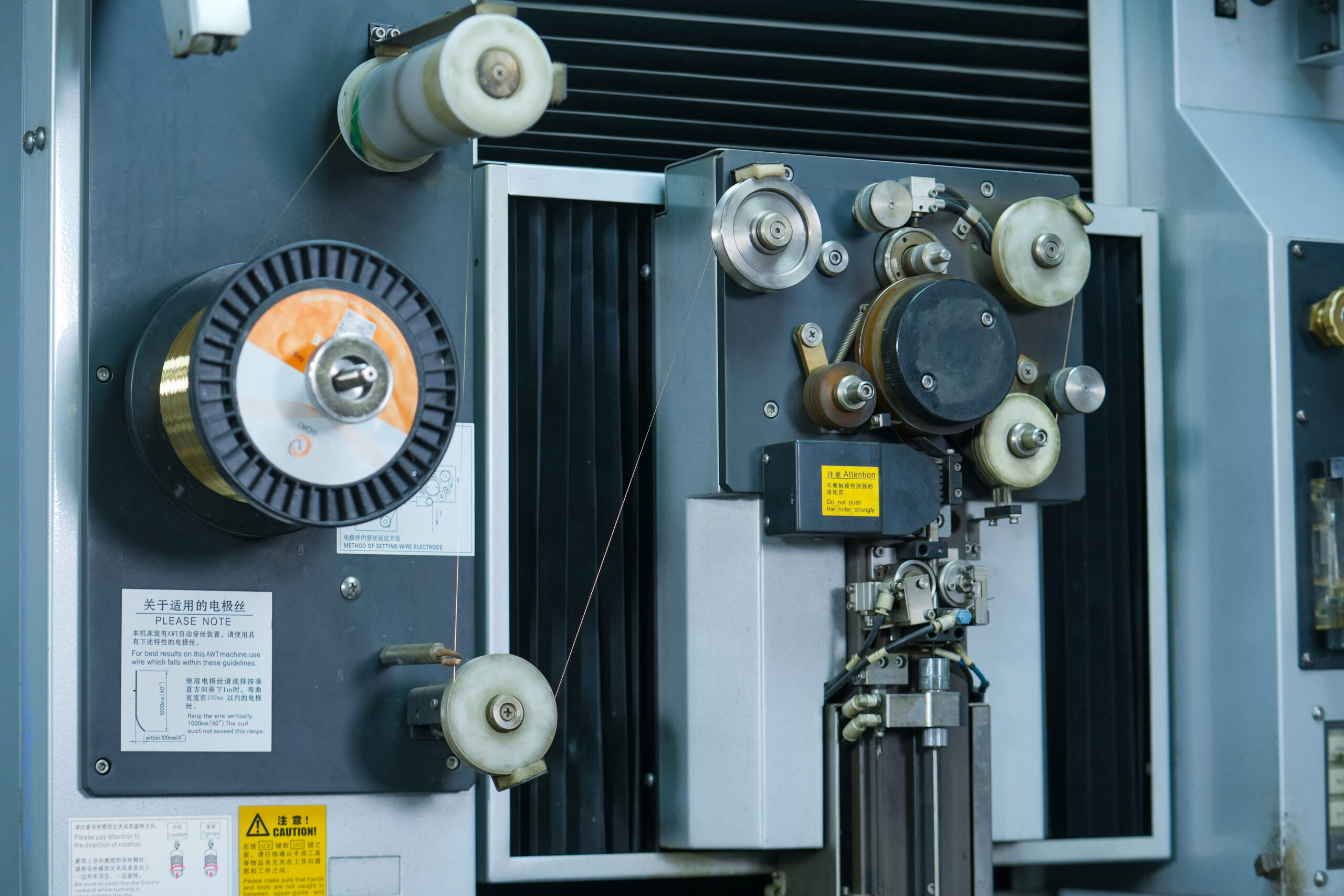
Yicen Precision addresses these challenges through strategic high-speed CNC machining with ball-end mills and specialized toolpaths that produce superior surface finishes directly from machining operations. Our 5-axis capabilities enable complex cavity geometries in minimal setups. EDM operations provide precision detail work for sharp corners, fine features, and areas inaccessible to cutting tools.
We employ proven heat treatment sequences with stress relieving between roughing and finishing operations to minimize distortion. Precision grinding of parting surfaces ensures flatness and parallelism specifications. Advanced polishing techniques including diamond paste and ultrasonic methods achieve mirror finishes. Our comprehensive quality control includes CMM inspection with detailed cavity dimension verification, surface profilometry for finish validation, and mold trial coordination to verify molding performance. Complete documentation supports ongoing production and future mold modifications.
D. Applications & Use Cases
Precision IC packaging molds manufactured by Yicen Precision serve critical roles across semiconductor packaging operations:
- QFN/DFN Package Molding – Quad flat no-lead and dual flat no-lead package molds
- BGA Package Production – Ball grid array mold tools for flip-chip and wire-bond assemblies
- SOIC/SOP Molding – Small outline integrated circuit package molds
- Power Module Packaging – High-power device encapsulation molds with thermal management
- System-in-Package (SiP) – Multi-die package molds for integrated systems
- Advanced Packaging – Fan-out wafer level package (FOWLP) and panel molding tools
- Automotive Electronics – Ruggedized package molds for automotive-grade components
E. Why Choose Yicen Precision for IC Packaging Molds?
Yicen Precision brings specialized expertise in semiconductor packaging tooling and mold manufacturing. Our engineering team collaborates with your packaging engineers to optimize mold designs through comprehensive DFM analysis. We evaluate gate locations, venting strategies, ejection systems, and cavity layouts to enhance moldability, reduce cycle time, and improve package quality.
Our prototype-to-production capabilities support initial mold validation through high-volume production tooling. Rapid turnaround times, typically 3-5 weeks for standard mold blocks depending on complexity, keep product launches on schedule. We provide complete material certifications and heat treatment documentation ensuring compliance with semiconductor packaging quality standards.
Cost-effective solutions result from efficient machining strategies, optimized tool steel selection, and design refinement without compromising the precision cavity accuracy and surface quality your packaging operations demand. Our mold maintenance and repair services extend tool life through refurbishment, repolishing, and modification capabilities. Whether you need single-cavity prototype molds or multi-cavity production tools, Yicen Precision delivers the reliability and precision that drives packaging yield. Request a technical consultation to discuss your specific IC packaging mold requirements.
 Skip to content