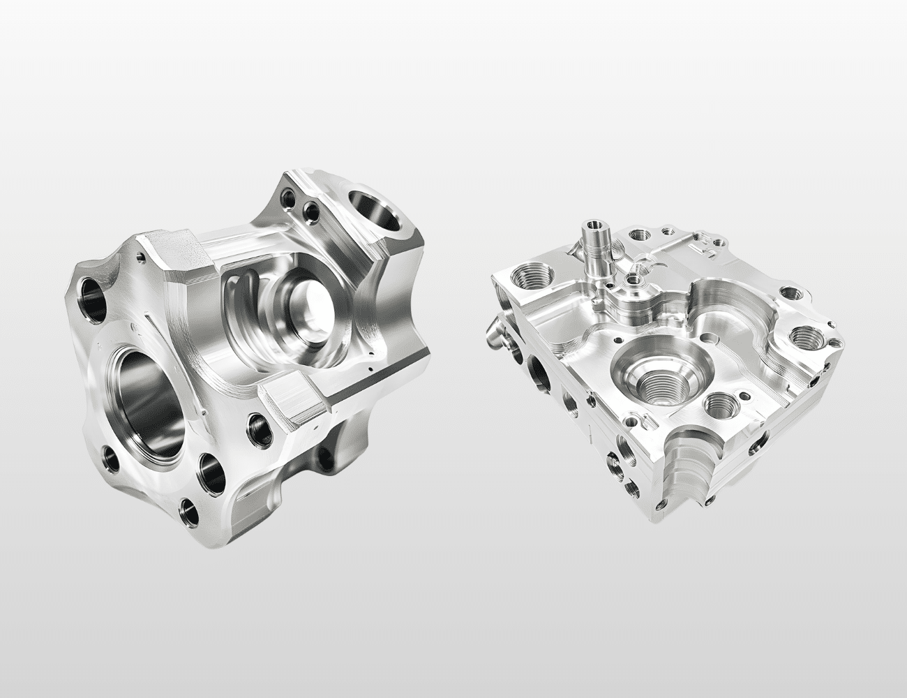
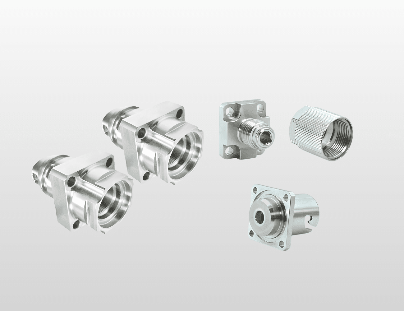
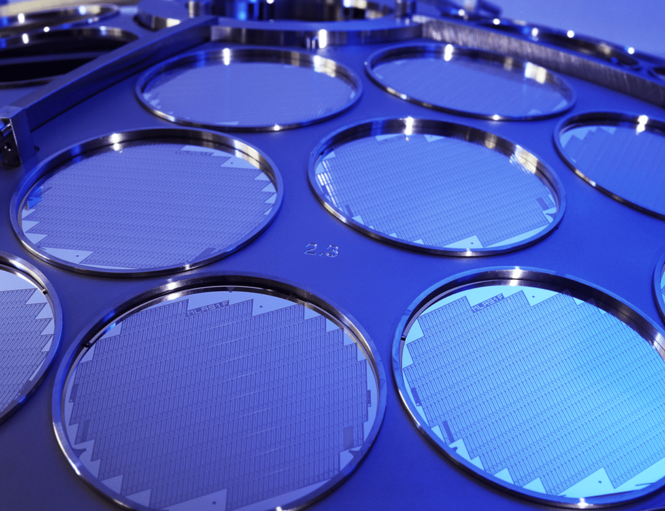
A. What are Vacuum Chamber Components?
Vacuum chamber components are specialized precision-engineered parts used in semiconductor manufacturing equipment to create and maintain ultra-high vacuum environments. These components include chamber bodies, flanges, viewports, feedthroughs, gate valves, and process modules that work together to achieve vacuum levels essential for semiconductor deposition, etching, and ion implantation processes. Used across wafer fabrication facilities, R&D laboratories, and semiconductor equipment manufacturing, vacuum chamber components must deliver absolute leak integrity, minimal outgassing, and contamination-free performance to ensure process reliability and product yield.
B. Wichtige technische Anforderungen
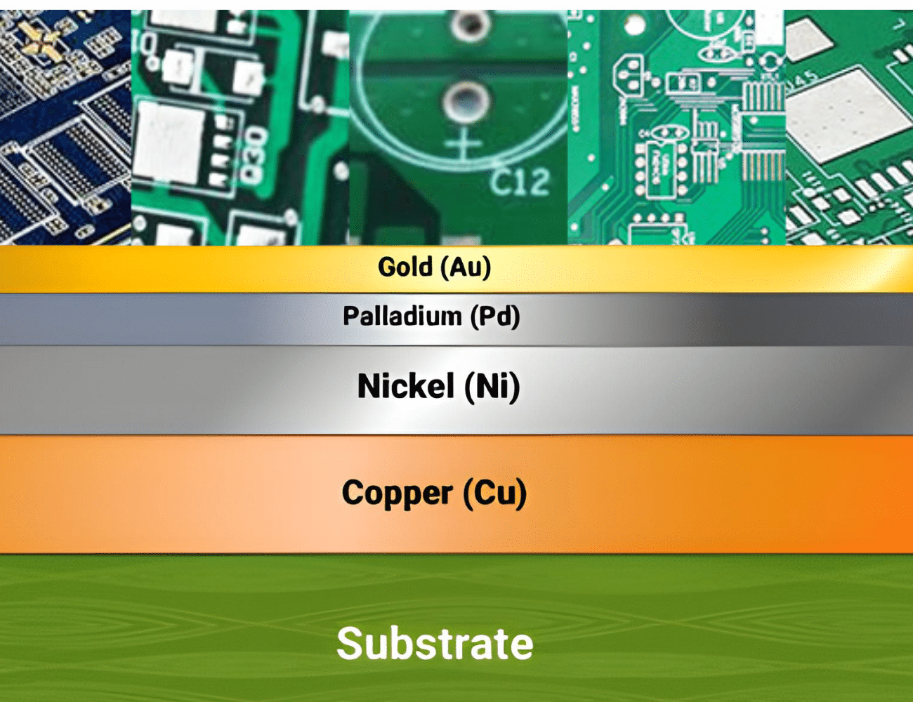
Vacuum chamber components for semiconductor applications demand exceptional precision and material properties. Tolerances of ±0.0005″ or tighter are standard for sealing surfaces and critical interfaces to ensure leak rates below 1×10⁻⁹ mbar·L/s. Surface finish requirements are stringent, with Ra values typically between 8-16 microinches for vacuum-sealing surfaces and even finer finishes for plasma-exposed areas.
Material specifications require low outgassing rates, corrosion resistance to process chemistries, and compatibility with plasma environments. Non-magnetic properties are often essential for applications involving magnetic fields. Components must withstand thermal cycling from cryogenic temperatures to 400°C while maintaining dimensional stability. Chemical compatibility with aggressive process gases, plasma resistance, and electropolishing capability are critical material considerations for long-term reliability.
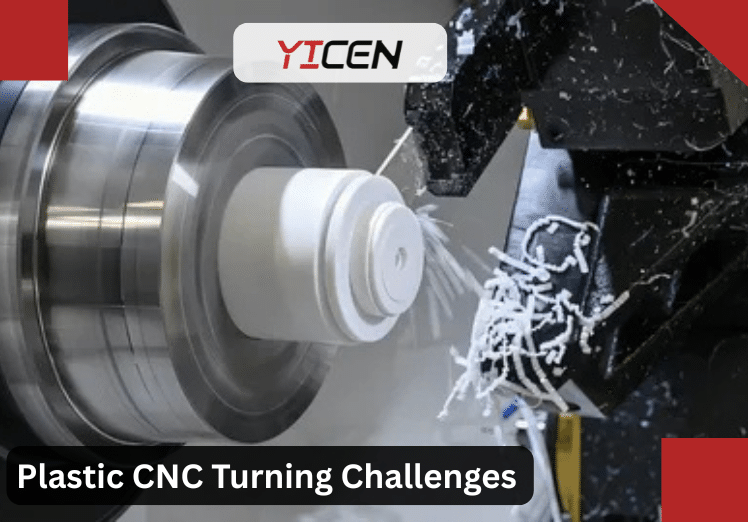
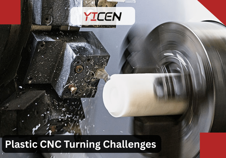
C. Herausforderungen und Lösungen bei der Herstellung
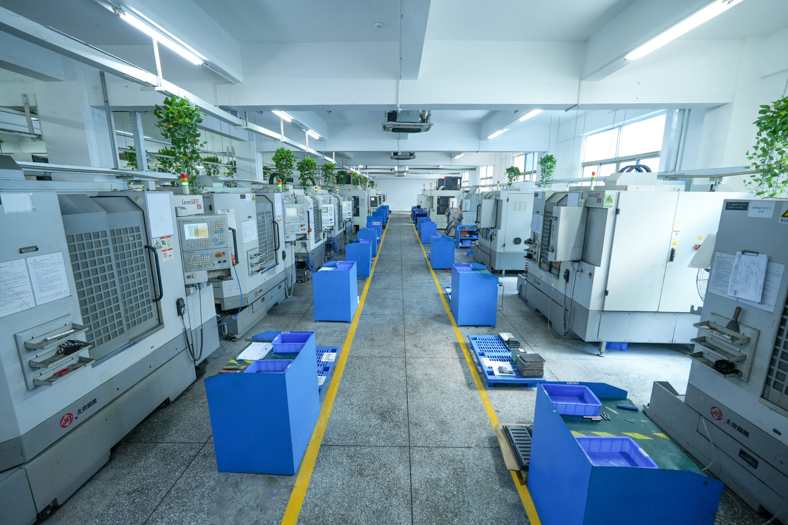
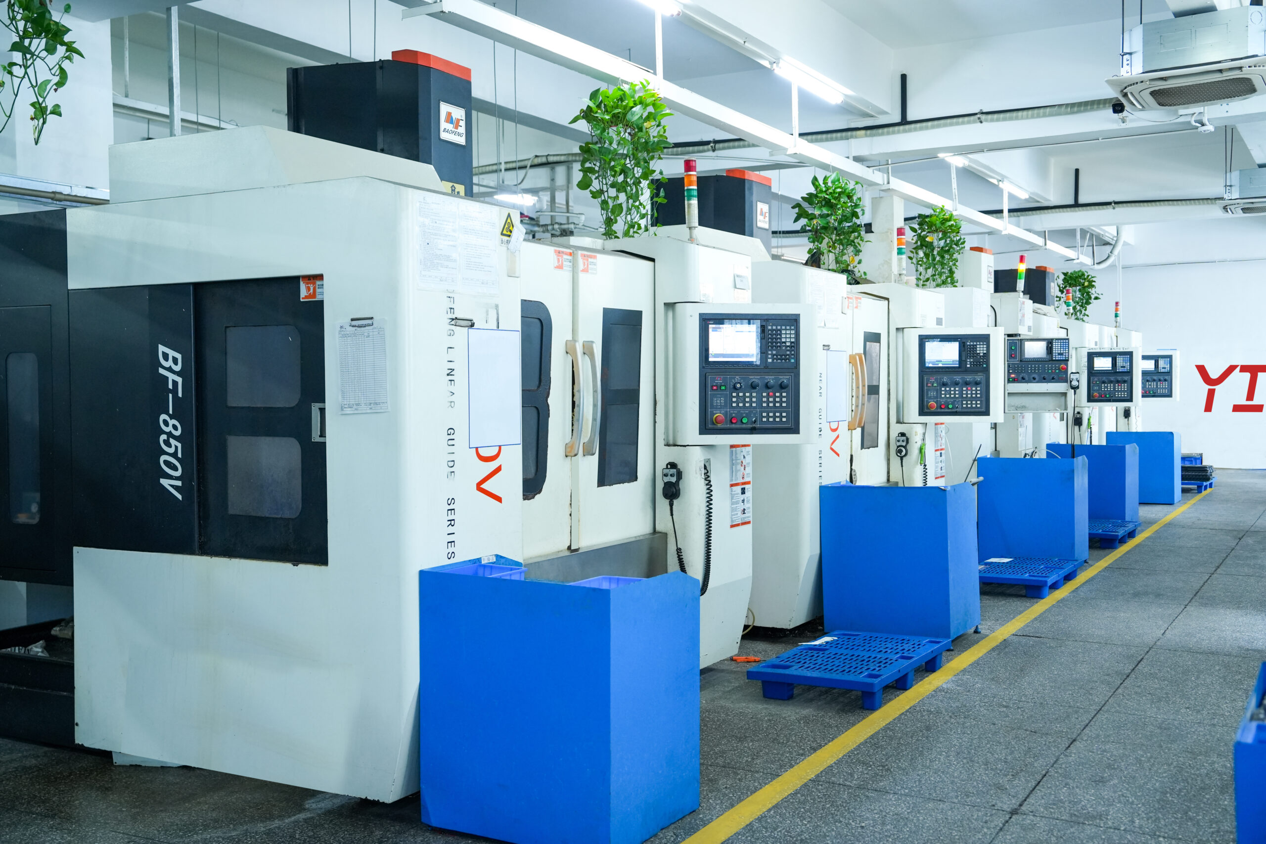
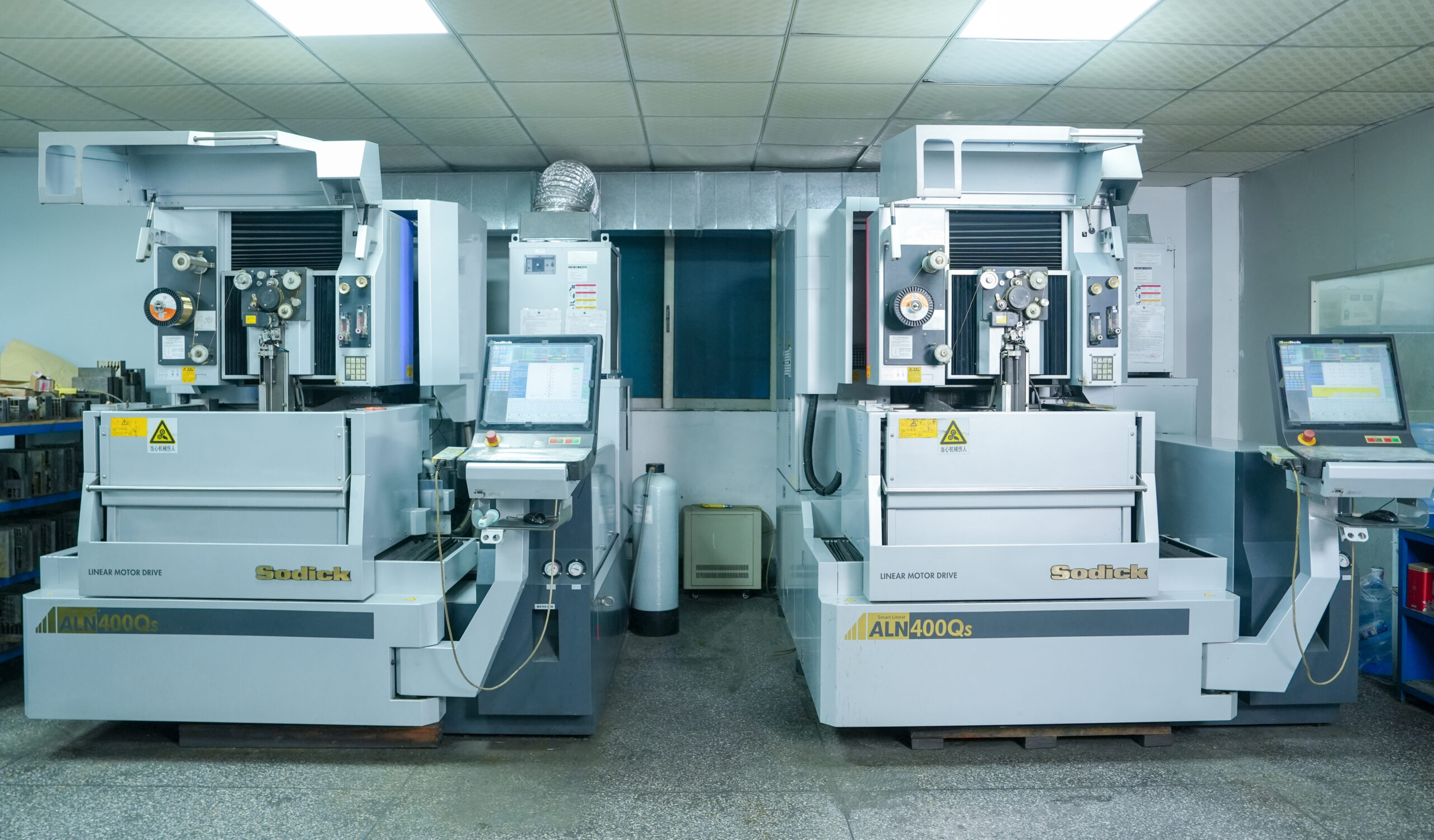
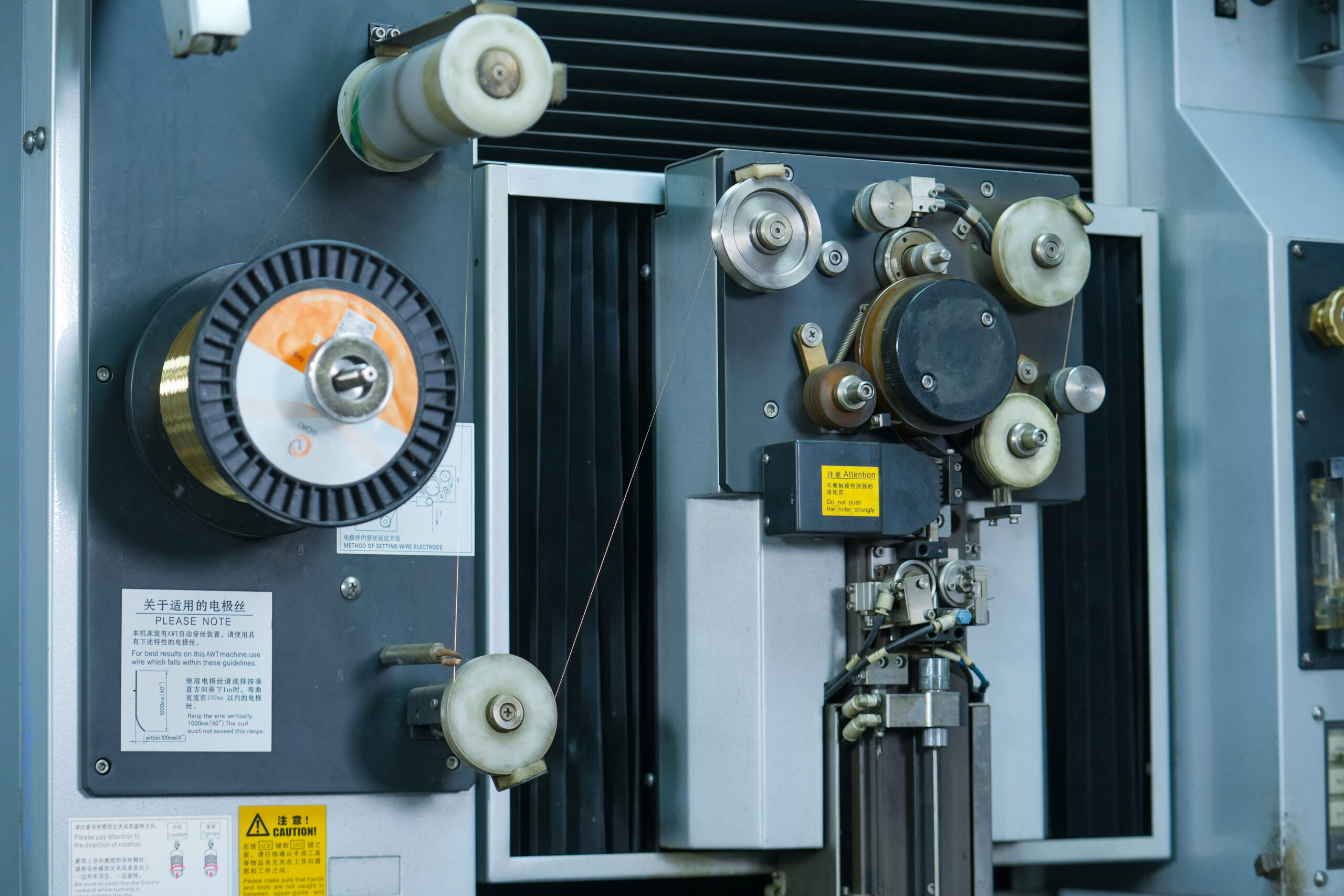
Machining vacuum chamber components presents unique challenges including achieving mirror-like surface finishes without subsurface damage, maintaining tight geometric tolerances across large chamber bodies, and eliminating microscopic surface defects that could compromise vacuum integrity. Material hardness, particularly with stainless steels and exotic alloys, requires specialized tooling strategies. Thin-walled sections demand precision fixturing to prevent distortion during machining.
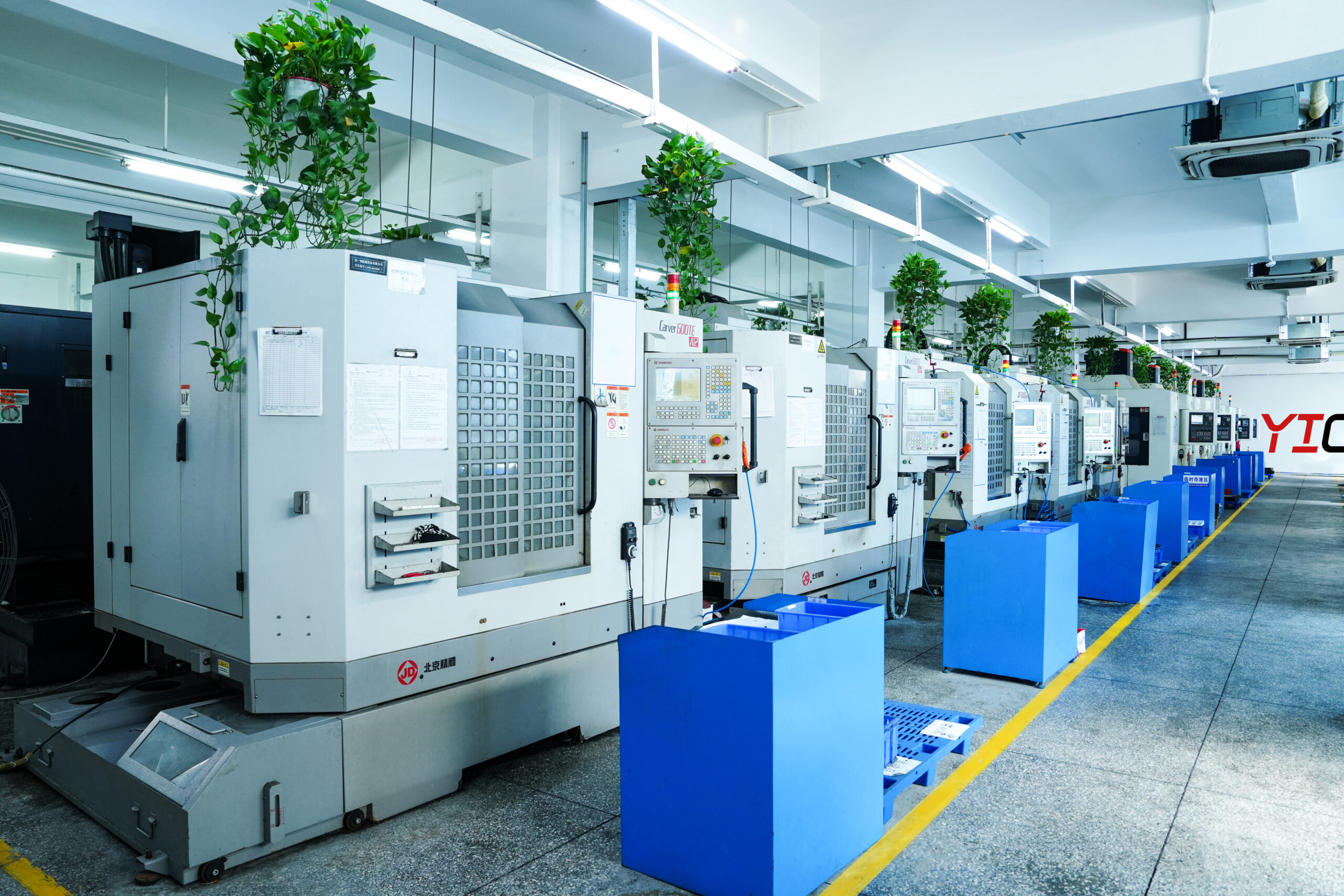
Yicen Precision overcomes these challenges through advanced 5-axis CNC machining that enables complex geometries in single setups, minimizing handling and improving accuracy. Our CAM software optimizes tool paths for superior surface finishes while our precision inspection tools verify every critical dimension. We employ specialized cutting tools designed for minimal work hardening and contamination.
Our comprehensive quality control includes CMM inspection for dimensional verification, surface profilometry for finish validation, and helium leak testing capability verification. We maintain cleanroom machining protocols to prevent particle contamination and use electropolishing partnerships for ultra-smooth final surfaces when required.
D. Anwendungen und Anwendungsfälle
Precision vacuum chamber components manufactured by Yicen Precision serve critical roles across semiconductor and advanced technology applications:
- Semiconductor Wafer Fabrication – PVD, CVD, and etching chamber assemblies
- Thin Film Deposition Systems – Sputtering and evaporation equipment chambers
- Ion Implantation Tools – Beam line chambers and process modules
- Plasma Processing Equipment – Reactive ion etching and plasma cleaning systems
- Semiconductor R&D Labs – Experimental vacuum systems and test chambers
- Analytical Instrumentation – Mass spectrometry and surface analysis equipment
- Display Manufacturing – OLED and flat panel production vacuum systems
E. Why Choose Yicen Precision for Vacuum Chamber Components?
Yicen Precision delivers unmatched expertise in semiconductor-grade vacuum chamber components machining. Our cleanroom-compatible manufacturing processes ensure contamination-free parts from initial machining through final packaging. We offer rapid prototyping to full production scalability, supporting both equipment manufacturers and research facilities with flexible volume capabilities.
Our engineering support includes DFM consultation to optimize designs for vacuum performance and manufacturability. Complete material traceability and certification documentation ensures compliance with semiconductor industry standards. We provide cost-effective solutions through efficient machining strategies and material utilization without compromising the ultra-high precision and surface quality demanded by vacuum applications.
Our experienced team understands the critical nature of vacuum integrity and process contamination control. Fast turnaround times, typically 2-4 weeks for complex components, keep your projects on schedule. Contact us for a custom quote tailored to your specific vacuum chamber component requirements.
 Zum Inhalt springen